Altium Designer 2025 - Schematic Editor - Customizing
Customize the schematic editor workspace to suit your unique needs
Customize the schematic editor workspace to suit your unique needs
Unlock the full potential of Altium Designer 2025 by personalizing the schematic editor interface according to your requirements. Optimize your workflow, configure hotkeys, and create the perfect environment for electronic circuit design.
Let's consider the categories of commands available for customization in the Schema Editor of Altium Designer.
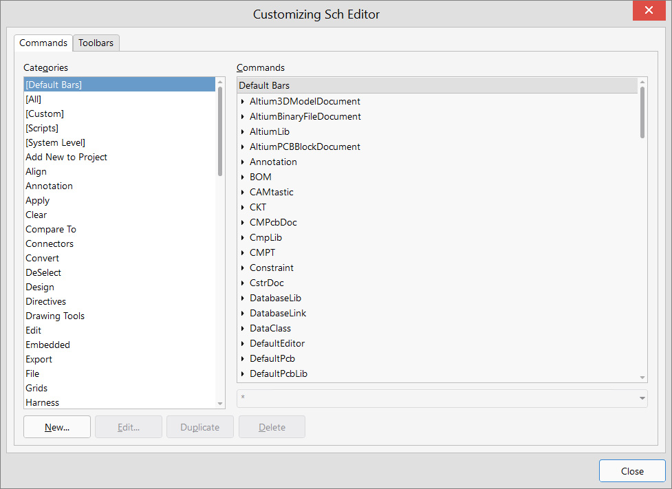
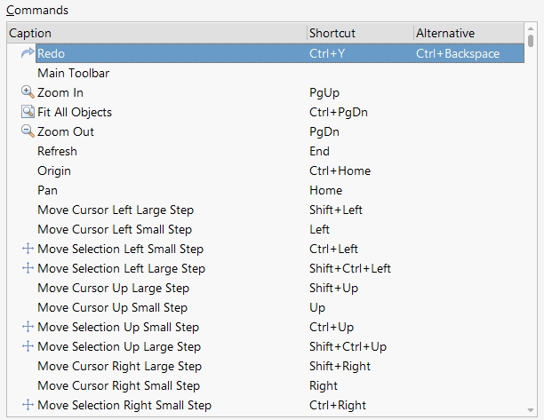
This "Customizing Sch Editor" dialog box allows users to customize toolbars and menus by adding or removing commands.
Here is an analysis of the command categories that can be seen in the screenshots:
Here is an analysis of the command categories that can be seen in the screenshots:
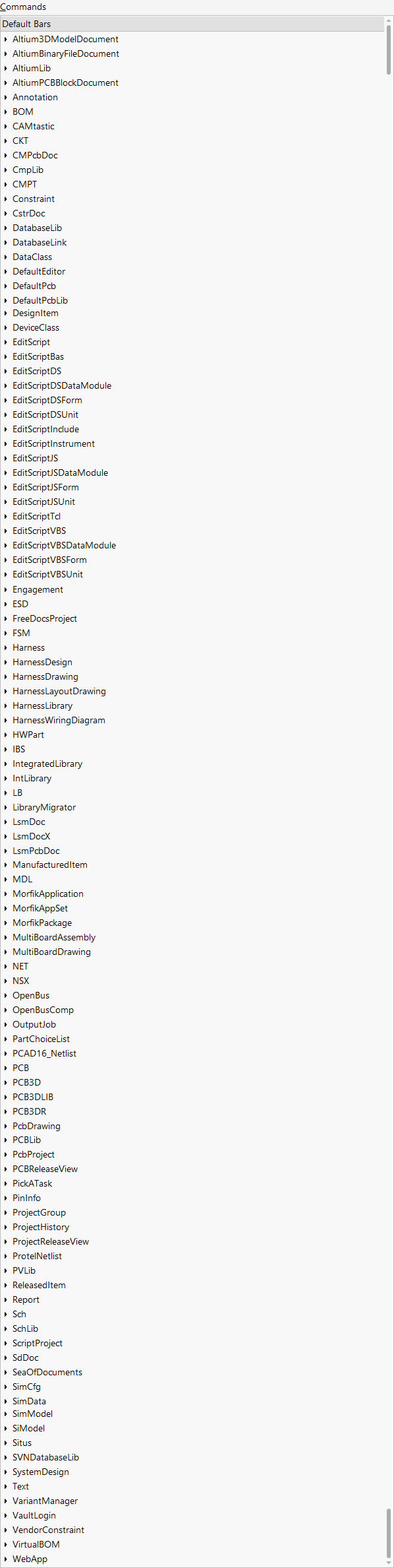
[Default Bars]: Contains commands that are already organized into standard Altium Designer toolbars (e.g., Standard, Utilities, Wiring, etc.). The right side of the window shows a list of these standard panels. Default Bars refers to the standard toolbar configurations and interface panels that are automatically displayed when the software launches. These are the basic UI elements (toolbars, menus, panels) that provide access to commonly used commands and functions, serving as the default workspace layout for users.Programming languages supported - DelphiScript as primary, VBScript and JavaScript as legacy options.
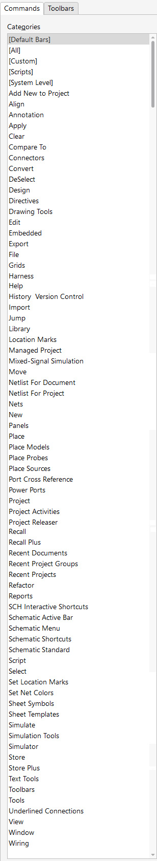
[System Level]: Commands relating to general program functions, system settings, licensing, and Altium Designer environment management. Add New to Project: Commands for creating and adding new documents to the current project (e.g., new schematic sheet, PCB, library, Output Job file, etc.). Align: Tools for aligning selected objects on the schematic (components, text, graphic elements) relative to each other or to the grid (e.g., align left, align top, distribute). Annotation: Commands for automatic or manual annotation (numbering) of components on the schematic (e.g., assigning reference designators R1, C1, U1). Apply: General "Apply changes" type commands, often associated with settings dialog boxes. Clear: Commands for clearing selections, filters, error markers (ERC), or other temporary information. Compare To: Tools for comparing the current document with another document or version, for example, to identify differences. Connectors: Commands specifically designed for placing and managing connector symbols. Convert: Tools for converting one type of object to another (e.g., selected primitives to a library component). DeSelect: Commands for deselecting objects (e.g., Deselect All, Deselect in Area). Design: Commands relating to project-level operations, such as project compilation, design rule checking (DRC) for schematics. Directives: Commands for placing and managing directives on the schematic (e.g., No ERC markers, directives for configuring net or class parameters). Drawing Tools: Commands for placing graphic primitives that are not electrical objects (lines, arcs, rectangles, text fields for comments). Edit: Standard editing commands: Cut, Copy, Paste, Delete, Undo, Redo, as well as editing object properties. Embedded: Commands related to embedded projects, such as FPGA development or embedded software links, if applicable to schematics. Export: Commands for exporting schematic data to various formats (e.g., PDF, images, netlists, CAD formats). File: Standard file operations: New, Open, Save, Save As, Print, Close. Grids: Commands for configuring and managing grids on the schematic (snap grid, visible grid). Harness: Tools for creating and managing signal harnesses and their elements (Harness Entries/Connectors). Help: Access to documentation, tutorials, program information. History Version Control: Commands for interacting with version control systems (e.g., Git, SVN), if configured. Import: Importing data into schematics (e.g., legacy format files, netlists, data from other CAD systems). Jump: Navigation commands (e.g., Go to Component, Go to Net, Go to Location Marker). Library: Commands related to schematic symbol libraries (opening, creating, managing, placing components from libraries). Location Marks: Tools for placing named markers on the schematic for quick navigation. Managed Project: Commands related to managed projects on Altium 365 or Concord Pro servers (e.g., check-in, check-out, synchronization). Mixed-Signal Simulation: Commands for setting up and running mixed analog-digital circuit simulation (if simulator tools are active/licensed). Move: Commands for moving selected objects. Netlist For Document: Generate netlist for the current schematic document. Netlist For Project: Generate netlist for the entire project. Nets: Commands for managing nets (highlighting, navigation, net properties). New: Similar to "Add New to Project", but may be more general or focused on creating new individual files. Panels: Commands for showing/hiding various interface panels (Projects, Libraries, Inspector, Messages, etc.). Place: Main category for placing electrical objects: Wires, Buses, Ports, Components, Power Ports, No ERC markers, directives, etc. Place Models: Placing models for simulation or possibly linking with footprints (although footprint placement typically occurs in PCB). In schematics, this most likely relates to simulation models. Place Probes: Placing probes for simulation (for measuring voltage, current, etc.). Place Sources: Placing voltage/current sources for simulation. Port Cross Reference: Tools for generating or managing cross-references for ports between hierarchical sheets. Power Ports: Commands for placing power port symbols (VCC, GND, etc.). Project: Project-level operations (Compile, Build, Project Options, Show Differences). Project Activities: Likely related to managed projects, change tracking, or tasks. Project Releaser: Commands for the project release process (generating manufacturing files, packaging). Recall: Possibly restoring previously saved views or settings. Recall Plus: Enhanced version of the "Recall" command. Recent Documents: Quick opening of recently accessed documents. Recent Project Groups: Quick opening of recent project groups. Recent Projects: Quick opening of recent projects. Refactor: Tools for controlled renaming of nets, components, or parameters throughout the project. Reports: Generation of various reports (Bill of Materials (BOM), component lists, netlists in report format). SCH Interactive Shortcuts: Commands that have standard keyboard shortcuts specific to the schematic editor. Schematic Active Bar: Commands typically found on the "Active Bar" (context-sensitive toolbar). Schematic Menu: Commands that populate the main menus of the schematic editor (File, Edit, View, etc.). Schematic Shortcuts: General keyboard shortcuts related to schematics. Schematic Standard: Commands typically found on the standard toolbar of the schematic editor. Script: (May be a duplicate or relate to specific script execution, as opposed to managing them) Possibly related to running specific, predefined scripts. Select: Commands for selecting objects (Select All, Select Inside Area, Select Objects Touching Line, etc.). Set Location Marks: Commands for defining location markers. Set Net Colors: Tools for assigning custom colors to nets for better visualization. Sheet Symbols: Commands for placing and managing sheet symbols for hierarchical design. Sheet Templates: Applying or managing templates for schematic sheets (e.g., borders, title blocks). Simulate: General simulation control commands (Run, Stop, Pause). Simulation Tools: Broader set of tools related to simulation setup and analysis. Simulator: Specific commands for interacting with the simulation engine. Store: Possibly saving current views or settings. Store Plus: Enhanced version of the "Store" command. Text Tools: Commands for manipulating text objects (font, size, alignment, find/replace text). Toolbars: Commands for showing/hiding specific toolbars. Tools: General category for utility commands that don't fit other categories (e.g., Cross Probe, Parameter Manager). Underlined Connections: Commands related to managing or visualizing connections that may be implicitly created (e.g., power nets connected by port names). View: Commands for controlling display (Zoom In, Zoom Out, Fit Document, Grids, Show/Hide elements). Window: Standard window management commands (Cascade, Tile, Switch Window). Wiring: Specific tools for placing electrical connections (Wires, Buses, Signal Harnesses).[Default Bars]: Contains commands that are already organized into standard Altium Designer toolbars (e.g., Standard, Utilities, Wiring, etc.). The right part of the window shows a list of these standard panels.
In this window, when you select [Default Bars] in the left pane of the Categories pane, the right pane of the Commands pane displays a list of the standard (built-in) toolbars and possibly menu structures that come with Altium Designer.Altium3DModelDocument - 3D model document for components
AltiumBinaryFileDocument - Binary file document format
AltiumLib - Altium library file
AltiumPCBDocument - PCB design document
Annotation - Component annotation and numbering
BOM - Bill of Materials generation
CAMtastic - CAM file viewer and editor
CKT - Circuit analysis tool
CMPubDoc - Component publishing document
CmpLib - Component library
CMPT - Component management
Constraint - Design rule constraints
CstDoc - Constraint document
DatabaseLib - Database library connection
DatabaseLink - Database linking functionality
DataClass - Data classification system
DefaultEditor - Default text editor
DefaultPcb - Default PCB template
DefaultPcbLib - Default PCB library
DesignItem - Design item management
DeviceClass - Device classification
EditScript - Script editing environment
EditScriptBas - Basic script editor
EditScriptDS - DelphiScript editor
EditScriptDSDataModule - DelphiScript data module editor
EditScriptDSForm - DelphiScript form editor
EditScriptDSUnit - DelphiScript unit editor
EditScriptInclude - Script include file editor
EditScriptInstrument - Script instrument editor
EditScriptJS - JavaScript editor
EditScriptJSDataModule - JavaScript data module editor
EditScriptJSForm - JavaScript form editor
EditScriptJSUnit - JavaScript unit editor
EditScriptTcl - Tcl script editor
EditScriptVBS - VBScript editor
EditScriptVBSDataModule - VBScript data module editor
EditScriptVBSForm - VBScript form editor
EditScriptVBSUnit - VBScript unit editor
Engagement - Project engagement tracking
ESO - Electronic sign-off
FreeDocProject - Free document project
FSM - Finite state machine
Harness - Cable harness design
HarnessDesign - Harness design environment
HarnessDrawing - Harness drawing creation
HarnessLayoutDrawing - Harness layout drawing
HarnessLibrary - Harness component library
HarnessWiringDiagram - Harness wiring diagram
HWPart - Hardware part definition
IBS - IBIS model support
IntegratedLibrary - Integrated component library
IntLibrary - Internal library
LB - Library browser
LibraryMigrator - Library migration tool
LsmDoc - LSM document format
LsmDocX - Extended LSM document
LsmPsbDoc - LSM PSB document
ManufacturerItem - Manufacturer part data
MDL - Model file format
ModelApplication - Model application
ModelAppSet - Model application set
ModelPackage - Model package
MultiBoardAssembly - Multi-board assembly design
MultiBoardDrawing - Multi-board drawing
NET - Netlist generation
NSK - Network socket
OpenBus - Open bus architecture
OpenBusComp - Open bus component
OutputJob - Output job configuration
PartChoiceList - Component selection list
PCAD16_Netlist - PCAD 16 netlist format
PCB - Printed circuit board design
PCB3D - 3D PCB visualization
PCB3DLib - 3D PCB component library
PCB3DR - 3D PCB renderer
PcbDrawing - PCB drawing
PCBLib - PCB component library
PcbProject - PCB project management
PCBReleaseView - PCB release view
PickAtTask - Pick and place task
PinInfo - Pin information
ProjectGroup - Project grouping
ProjectHistory - Project version history
ProjectReleaseView - Project release view
ProtelNetlist - Protel netlist format
PVLib - Parameter validation library
ReleaseItem - Release item management
Report - Report generation
Sch - Schematic design
SchLib - Schematic library
ScriptProject - Scripting project
SiDoc - Signal integrity document
SilkOlDocuments - Silkscreen overlay documents
SimCfg - Simulation configuration
SimData - Simulation data
SimModel - Simulation model
SMModel - Signal model
Slug - Design slug
SVNDatabaseLib - SVN database library
SystemDesign - System-level design
Test - Test configuration
VariantManager - Design variant management
VaultLogin - Vault system login
VendorConstraint - Vendor constraint
VirtualBOM - Virtual bill of materials
WebApp - Web application interface
[All]: This category displays absolutely all available commands for the schematic editor in one long list, without grouping. Useful if you're looking for a specific command but don't know which category it belongs to.
[Custom]: This is where user-created commands will be displayed, for example, through scripts or macros that have been added to the interface.
[Scripts]: Commands related to running and managing scripts (e.g., VBScript, JScript, DelphiScript) that automate tasks in Altium Designer.
[System Level]: Commands related to general program functions, system settings, licensing, and management of the Altium Designer environment.
Add New to Project: Commands for creating and adding new documents to the current project (e.g., new schematic sheet, PCB, library, Output Job file, etc.).
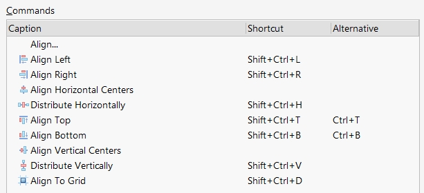
Align: Tools for aligning selected objects on the schematic (components, text, graphic elements) relative to each other or the grid (e.g., align left, align top, distribute).
Align Left (Shift+Ctrl+L) - Aligns all selected objects to the leftmost position of the selection
Align Right (Shift+Ctrl+R) - Aligns all selected objects to the rightmost position
Align Horizontal Centers - Centers all selected objects horizontally relative to each other
Distribute Horizontally (Shift+Ctrl+H) - Evenly spaces selected objects horizontally between the leftmost and rightmost objects
Align Top (Shift+Ctrl+T or Ctrl+T) - Aligns all selected objects to the topmost position
Align Bottom (Shift+Ctrl+B or Ctrl+B) - Aligns all selected objects to the bottommost position
Align Vertical Centers - Centers all selected objects vertically relative to each other
Distribute Vertically (Shift+Ctrl+V) - Evenly spaces selected objects vertically between the topmost and bottommost objects
Align To Grid (Shift+Ctrl+D) - Snaps all selected objects to the nearest grid points
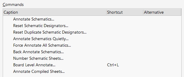
Annotation: Commands for automatic or manual annotation (numbering) of components on the schematic (e.g., assigning designators R1, C1, U1).
Core Annotation:
Annotate Schematics... - Opens the main annotation dialog to automatically assign designators to components based on rules and settings you define
Annotate Schematics Quietly... - Performs annotation automatically without showing the dialog, using previously saved settings
Force Annotate All Schematics... - Forces re-annotation of ALL components, even those already annotated, across all schematic sheets
Reset Commands:
Reset Schematic Designators... - Removes all designators from components, returning them to their original state (like R?, C?, U?)
Reset Duplicate Schematic Designators... - Only resets components that have duplicate designators, useful for fixing numbering conflicts
Advanced Annotation:
Back Annotate Schematics... - Updates schematic designators to match those from the PCB layout (when changes were made on the PCB side)
Board Level Annotate... (Ctrl+L) - Performs annotation at the PCB level, typically used when working with the board layout
Annotate Compiled Sheets... - Annotates components in compiled/flattened schematic sheets
Sheet Management:
Number Schematic Sheets... - Assigns sequential numbers to multiple schematic sheets in your project
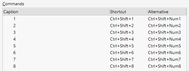
Apply: General commands such as "Apply changes," often associated with settings dialog boxes.
Apply Commands Overview
These are general commands for "Apply changes," typically associated with settings dialog boxes. They provide quick shortcuts to apply different types of modifications or settings.
Apply Command Structure:
Numbered Commands (1-8):
Command 1 (Ctrl+Shift+1 or Ctrl+Shift+Num1)
Command 2 (Ctrl+Shift+2 or Ctrl+Shift+Num2)
Command 3 (Ctrl+Shift+3 or Ctrl+Shift+Num3)
Command 4 (Ctrl+Shift+4 or Ctrl+Shift+Num4)
Command 5 (Ctrl+Shift+5 or Ctrl+Shift+Num5)
Command 6 (Ctrl+Shift+6 or Ctrl+Shift+Num6)
Command 7 (Ctrl+Shift+7 or Ctrl+Shift+Num7)
Command 8 (Ctrl+Shift+8 or Ctrl+Shift+Num8)
How These Work:
Purpose: These numbered Apply commands serve as quick shortcuts to:
Apply specific sets of parameters or settings
Execute frequently used operations without opening full dialog boxes
Apply different types of changes based on the current context (schematic editing, component placement, etc.)
Context-Sensitive: The actual function of each numbered command depends on what you're currently doing in Altium Designer - they adapt to the active tool or dialog.
Efficiency: Instead of going through multiple dialog steps, you can quickly apply common changes using these keyboard shortcuts.
Customizable: These commands can typically be customized to perform specific operations that you use frequently in your design workflow.
This system allows experienced users to work much faster by avoiding repetitive dialog navigation for common operations.
Clear: Commands for clearing selections, filters, error markers (ERC), or other temporary information.
Let me explain the Clear commands in Altium Designer 2025:
Clear Commands Overview
These commands are for clearing selections, filters, error markers (ERC), or other temporary information from your design workspace.
Clear Command Structure:
Numbered Commands (1-8):
Clear Command 1
Clear Command 2
Clear Command 3
Clear Command 4
Clear Command 5
Clear Command 6
Clear Command 7
Clear Command 8
Typical Clear Functions:
Common Clear Operations:
Clear Selection - Deselects all currently selected objects
Clear Filters - Removes active filtering criteria applied to components or nets
Clear ERC Markers - Removes Electrical Rule Check error/warning markers from the schematic
Clear Violations - Clears design rule violation markers
Clear Highlights - Removes highlighting from nets, components, or other objects
Clear Search Results - Clears results from find/search operations
Clear Temporary Graphics - Removes temporary drawing elements or measurement lines
Clear Annotations - Removes temporary notes or markup
Purpose and Benefits:
Clean Workspace: Quickly clean up your design view by removing temporary visual elements
Reset State: Return the schematic to a clean state without temporary markers or selections
Performance: Clear unnecessary visual information that might slow down screen updates
Focus: Remove distractions to focus on specific design areas
Usage Context:
These commands are particularly useful during design review, debugging, or when switching between different analysis tasks where you want to start with a clean visual slate.
Compare To: Tools for comparing the current document with another document or version, for example, to detect differences.
Let me explain the Compare To commands in Altium Designer 2025:
Compare To Commands Overview
These tools allow you to compare the current document with another document or version to detect differences - essential for version control and change tracking.
Individual Compare Commands:
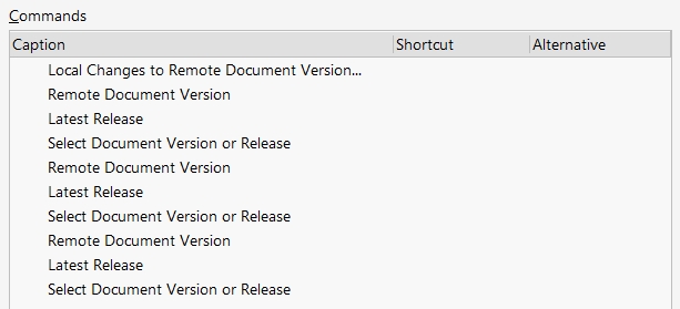
Version Comparison:
Local Changes to Remote Document Version... - Compares your local working copy with the remote repository version to see what changes you've made
Remote Document Version - Compares with a specific version stored in the remote repository
Latest Release - Compares your current document with the most recent released version
Selection Options:
Select Document Version or Release - Opens a dialog to choose which specific version or release you want to compare against
Key Comparison Features:
What Gets Compared:
Component changes (added, removed, modified)
Net connectivity differences
Parameter modifications
Schematic layout changes
Symbol updates
Visual Differences:
Highlights changed objects in different colors
Shows additions, deletions, and modifications
Provides detailed change reports
Typical Use Cases:
Version Control: Track what's changed between design revisions
Collaboration: See differences when multiple engineers work on the same design
Quality Control: Verify changes match intended modifications
Release Management: Compare working version against released designs
Troubleshooting: Identify when specific changes were introduced
Workflow:
Open your current schematic
Choose appropriate Compare To command
Select target version/document to compare against
Review highlighted differences in the comparison view
Accept, reject, or document the changes as needed
This is crucial for maintaining design integrity in team environments and version-controlled projects.
Connectors: Commands specifically designed for placing and managing connector symbols.
Let me explain the Connectors commands in Altium Designer 2025:
Connectors Commands Overview
These commands are specifically designed for placing and managing connector symbols that represent electrical connections in your schematic design.
Individual Connector Commands:
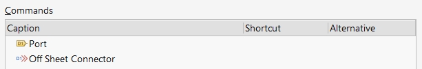
Port
Places a port symbol on the schematic
Ports are used to define connection points that can connect to other schematic sheets or hierarchical blocks
Essential for creating modular, hierarchical designs
Allows signals to flow between different levels of your design hierarchy
Commonly used in top-level schematics to interface with sub-circuits
Off Sheet Connector
Places an off-sheet connector symbol
Used to represent connections that continue on different pages/sheets of the same schematic
Helps keep schematics clean by avoiding long wires that would span across multiple sheets
Two off-sheet connectors with the same name automatically connect electrically
Useful for complex designs spread across multiple schematic pages
Key Uses:
Design Organization:
Break complex circuits into manageable, readable sections
Connect signals across multiple schematic sheets
Create clean interfaces between different circuit blocks
Hierarchy Management:
Ports enable hierarchical design methodology
Allow parent sheets to communicate with child sheets
Essential for modular circuit design
Documentation:
Off-sheet connectors clearly show where signals continue
Reduce wire clutter on individual schematic pages
Maintain electrical connectivity while improving readability
Typical Workflow:
Use Port for hierarchical connections between schematic levels
Use Off Sheet Connector for connections that span multiple pages of the same hierarchical level
Name connectors consistently to ensure proper electrical connection
Verify connections using design rule checks
These tools are essential for organizing complex, multi-page schematic designs effectively.
Convert: Tools for converting one type of object to another (e.g., selected primitives into a library component).
Let me explain the Convert commands in Altium Designer 2025:
Convert Commands Overview
These tools convert one type of object to another, such as converting selected primitives into library components or transforming design elements between different formats.
Individual Convert Commands:
Component/Part Conversion:
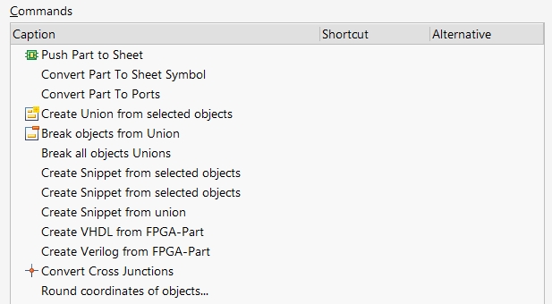
Push Part to Sheet - Pushes a component from the current sheet to another sheet in the hierarchy
Convert Part To Sheet Symbol - Converts a regular component into a sheet symbol for hierarchical design
Convert Part To Ports - Transforms a component into individual port connections
Object Grouping:
Create Union from selected objects - Combines multiple selected objects into a single union object
Break objects from Union - Separates objects that were previously grouped in a union
Break all objects Unions - Dissolves all union groupings in the current sheet
Code Generation:
Create VHDL from FPGA-Part - Generates VHDL code from FPGA component definitions
Create Verilog from FPGA-Part - Generates Verilog code from FPGA component definitions
Snippet Management:
Create Snippet from selected objects - Converts selected elements into reusable design snippets
Create Snippet from union - Creates a snippet from a union of objects
Wire/Connection Conversion:
Convert Cross Junctions - Converts wire crossing points between different junction types (T-junctions, cross-junctions, etc.)
Coordinate Processing:
Round coordinates of objects... - Rounds object coordinates to specified precision, useful for cleaning up designs
Key Benefits:
Design Reuse: Convert custom drawings into reusable library components
Hierarchy Management: Transform components for different levels of design hierarchy
Code Generation: Automatically create HDL code from schematic components
Organization: Group related objects or break them apart as needed
Clean-up: Standardize coordinates and junction types for consistency
These conversion tools are essential for maintaining organized, reusable, and manufacturable designs.
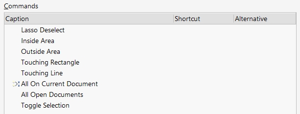
DeSelect: Commands for deselecting objects (e.g., Deselect All, Deselect in Area).
DeSelect Commands Overview
These commands provide various ways to deselect objects, giving you precise control over what remains selected in your schematic design.
Individual DeSelect Commands:
Selection Methods:
Lasso Deselect - Deselects objects by drawing a freeform lasso around them
Inside Area - Deselects all objects that are completely inside a defined rectangular area
Outside Area - Deselects all objects that are completely outside a defined area
Touching Rectangle - Deselects objects that touch or intersect with a rectangular selection area
Touching Line - Deselects objects that touch or cross a drawn line
Scope-Based Deselection:
All On Current Document - Deselects all objects on the currently active schematic sheet
All Open Documents - Deselects all objects across all currently open schematic documents
Toggle Selection - Inverts the current selection (selected objects become deselected, deselected objects become selected)
Key Benefits:
Precision Control: Fine-tune your selection by removing specific objects from a larger selection set
Workflow Efficiency: Quickly clear selections without starting over from scratch
Complex Operations: Combine with Select commands to create sophisticated selection patterns
Multi-Document Management: Handle selections across multiple open schematics simultaneously
Typical Use Cases:
Refining Selections: Start with a broad selection, then deselect unwanted objects
Incremental Selection: Build complex selections by adding and removing objects iteratively
Area-Based Operations: Work with objects in specific regions while excluding others
Batch Operations: Prepare precise object sets for bulk modifications
Workflow Example:
Select a large area of components
Use "Inside Area" to deselect components you don't want to modify
Perform operations only on the remaining selected objects
These commands provide the flexibility needed for complex selection operations in professional schematic design.
Design: Commands related to project-level operations, such as project compilation, design rule checking (DRC) for schematics.
Design Commands Overview
These commands handle project-level operations including project compilation, design rule checking (DRC), library management, and hierarchical design operations.
Individual Design Commands:
Project Updates:
Update Schematic... (multiple entries) - Updates and compiles schematic documents, resolving component references and checking connectivity
Import Operations:
Import Schematic... - Imports schematic files from other formats or projects
Import Wiring Diagram... - Imports wiring diagrams and converts them to schematic format
Constraint Management:
Constraint Manager... - Opens the constraint management system for defining design rules and parameters
Migrate Project to Constraint Manager Flow... - Converts older projects to use the modern constraint management system
Library Operations:
Browse Library... - Opens library browser to view and manage component libraries
Make Schematic Library - Creates a schematic symbol library from current design
Make Integrated Library - Combines schematic and PCB libraries into a single integrated library
Hierarchical Design Management:
Create Sheet From Sheet Symbol - Generates a new schematic sheet based on an existing sheet symbol
Create Sheet Symbol From Sheet - Creates a hierarchical sheet symbol from an existing schematic sheet
Create Component From Sheet - Converts a schematic sheet into a reusable component
Rename Child Sheet... - Renames hierarchical child sheets in the project
Synchronize Sheet Entries and Ports - Ensures consistency between hierarchical sheet interfaces and their corresponding ports
Key Functions:
Project Compilation: Ensures all design elements are properly linked and validated
Design Verification: Checks for electrical and design rule violations
Library Management: Creates and maintains component libraries
Hierarchical Design: Manages complex multi-sheet designs with proper hierarchy
Import/Export: Integrates with other design tools and formats
These commands are essential for managing complex, professional electronic design projects from conception through completion.

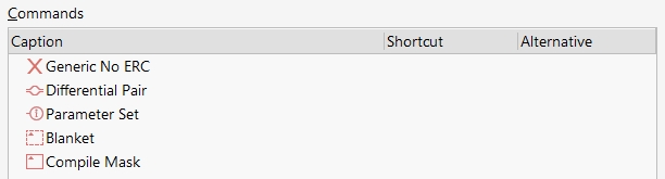
Directives: Commands for placing and managing directives on the schematic (e.g., No ERC markers, directives for configuring network parameters or classes).
Directives Commands Overview
These commands place special directive objects on the schematic that control design compilation, error checking, signal processing, and network parameter configuration.
Individual Directive Commands:
Error Control:
Generic No ERC - Places a directive that suppresses Electrical Rule Check (ERC) errors at specific locations
Used when you intentionally want to ignore certain ERC violations
Prevents false error reports for legitimate design choices
Can be configured to suppress specific types of ERC violations
Signal Management:
Differential Pair - Defines pairs of signals as differential pairs for high-speed design
Critical for maintaining signal integrity in high-frequency circuits
Ensures proper routing and spacing in PCB layout
Used for signals like LVDS, USB, Ethernet, etc.
Parameter Control:
Parameter Set - Sets specific parameters for components, nets, or design regions
Controls electrical characteristics like impedance, timing, voltage levels
Defines routing constraints and design rules
Customizes component behavior for simulation
Design Compilation:
Blanket - Places a blanket directive that can suppress multiple types of warnings or errors over a defined area
Useful for prototype or experimental circuit sections
Prevents compilation warnings in specific design regions
Compile Mask - Masks certain areas from compilation processing
Excludes specific circuit sections from design rule checking
Useful for legacy circuits or third-party IP blocks
Key Benefits:
Design Intent Control: Clearly document intentional design decisions that might otherwise trigger warnings
Signal Integrity: Properly define high-speed signal requirements
Compilation Management: Control which parts of the design are processed and how
Error Suppression: Eliminate false positives while maintaining design rule integrity
These directives are essential for professional designs where you need precise control over design rules and compilation behavior.
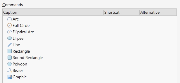
Drawing Tools: Commands for placing graphic primitives that are not electrical objects (lines, arcs, rectangles, text fields for comments).
Drawing Tools Commands Overview
These commands place graphic primitives that are non-electrical objects used for documentation, visual enhancement, and annotation of schematics.
Individual Drawing Tool Commands:
Curved Objects:
Arc - Draws a curved arc segment between two points with specified radius
Full Circle - Creates a complete circular shape
Elliptical Arc - Draws an arc segment of an ellipse (stretched circle)
Ellipse - Creates an oval/elliptical shape
Straight Line Objects:
Line - Draws straight line segments for borders, dividers, or annotations
Bezier - Creates smooth curved lines using Bezier curve control points
Geometric Shapes:
Rectangle - Draws rectangular shapes with sharp corners
Round Rectangle - Creates rectangles with rounded corners
Polygon - Draws multi-sided shapes with any number of vertices
Advanced Graphics:
Graphic... - Places more complex graphical objects or imported images
Key Characteristics:
Non-Electrical: These objects don't participate in electrical connectivity or netlist generation
Documentation Purpose: Used for:
Circuit block outlines and groupings
Schematic borders and frames
Explanatory diagrams and flowcharts
Company logos and branding
Notes and callout shapes
Visual separation of circuit sections
Customizable Properties:
Line width and style
Fill colors and patterns
Layer assignment
Transparency settings
Common Uses:
Organization: Group related components visually with rectangles or polygons
Documentation: Add explanatory diagrams alongside electrical circuits
Presentation: Enhance schematic appearance for reports and presentations
Annotation: Create callouts and highlighting for design reviews
These tools help create professional, well-documented schematics that clearly communicate design intent beyond just electrical connectivity.
Edit: Standard editing commands: Cut, Copy, Paste, Delete, Undo, Redo, as well as editing object properties.
Edit Commands Overview
Standard editing commands for Cut, Copy, Paste, Delete, Undo, Redo, plus specialized editing functions for object properties and schematic-specific operations.
Individual Edit Commands:
Basic Editing:
Undo (Ctrl+Z, Alt+Backspace) - Reverses the last action performed
Redo (Ctrl+Y, Ctrl+Backspace) - Re-applies the last undone action
Cut (Ctrl+X, Shift+Delete) - Removes selected objects and places them in clipboard
Copy (Ctrl+C, Ctrl+Insert) - Copies selected objects to clipboard without removing them
Copy As Text - Copies object information as text format for external use
Paste Operations:
Paste (Ctrl+V, Shift+Insert) - Places clipboard contents at cursor location
Smart Paste... (Ctrl+Shift+V) - Advanced paste with options for positioning and properties
Search and Replace:
Find Text... (Ctrl+F) - Searches for specific text within the schematic
Replace Text... (Ctrl+H, Ctrl+G) - Finds and replaces text strings throughout the design
Find Next (F3) - Continues to next occurrence of current search term
Object Management:
Delete - Removes selected objects permanently
Duplicate (Ctrl+R) - Creates copies of selected objects with smart positioning
Find Similar Objects (Shift+F) - Selects all objects with similar properties to the current selection
Schematic-Specific:
Break Wire - Splits a wire at the cursor location, useful for inserting components
Increment Part Number - Automatically increments component designators (R1→R2, etc.)
Key Benefits:
Efficiency: Standard keyboard shortcuts work as expected
Smart Operations: Duplicate and Smart Paste understand schematic context
Search Power: Find/Replace works across entire projects
Wire Management: Break Wire enables easy circuit modifications
These commands form the foundation for efficient schematic editing workflows in professional electronic design.

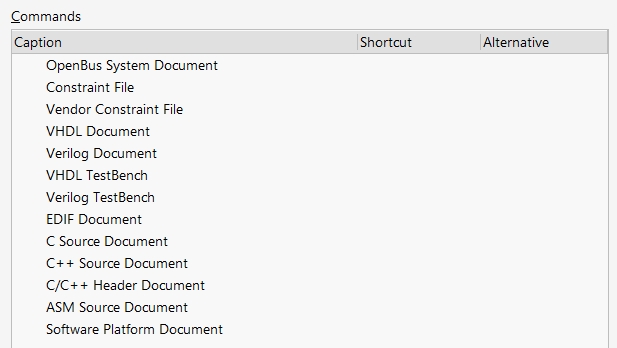
Embedded: Commands related to embedded projects, such as FPGA development or connections with embedded software, if applicable to schematics.
Embedded Commands Overview
These commands handle embedded projects including FPGA development, HDL design, and connections with embedded software development within the Altium environment.
Individual Embedded Commands:
System Integration:
OpenBus System Document - Creates system-level documents for defining embedded system architecture and bus connections
Software Platform Document - Defines the software platform and runtime environment for embedded processors
FPGA Design Files:
VHDL Document - Creates VHDL hardware description language files for FPGA logic design
Verilog Document - Creates Verilog HDL files for FPGA development
VHDL TestBench - Generates VHDL simulation testbench files for design verification
Verilog TestBench - Creates Verilog simulation testbench files for testing logic designs
Constraint Management:
Constraint File - Creates timing and placement constraint files for FPGA compilation
Vendor Constraint File - Generates vendor-specific constraint files (Xilinx, Intel/Altera, etc.)
Netlist and Integration:
EDIF Document - Creates Electronic Design Interchange Format files for FPGA tool integration
Software Development:
C Source Document - Creates C language source code files for embedded processors
C++ Source Document - Generates C++ source files for embedded applications
C/C++ Header Document - Creates header files for C/C++ embedded software
ASM Source Document - Generates assembly language files for low-level embedded programming
Key Benefits:
Unified Environment: Develop both hardware schematics and FPGA/embedded software in one tool
Hardware-Software Co-Design: Seamlessly integrate FPGA logic with embedded processors
Simulation Support: Generate testbenches for design verification
Multi-Vendor Support: Create constraint files for different FPGA vendors
Complete Workflow: From schematic capture through FPGA implementation and embedded software
These commands enable comprehensive embedded system development combining traditional circuit design with programmable logic and embedded software development.
Export: Commands for exporting schematic data to various formats (e.g., PDF, images, netlists, CAD formats).
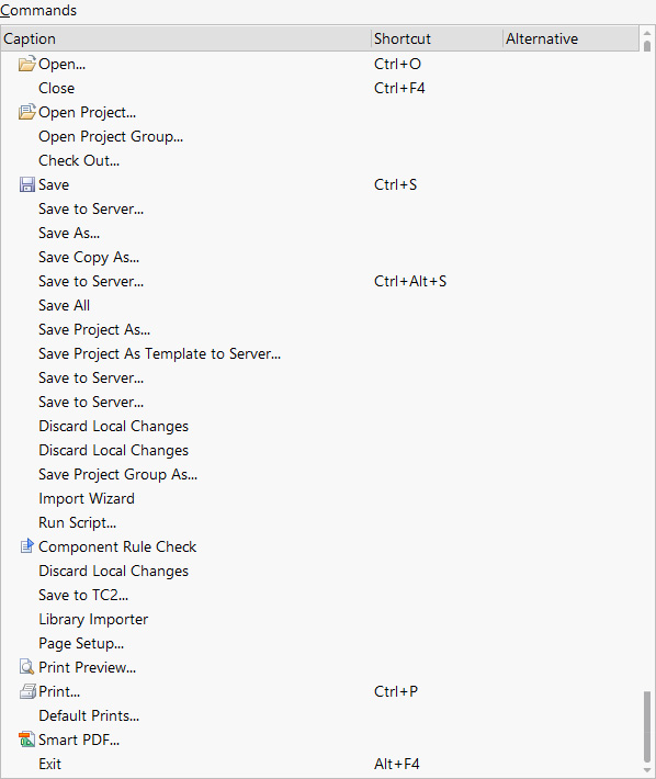
File: Standard file operations: New, Open, Save, Save As, Print, Close.
Let me explain the File commands in Altium Designer 2025:
File Commands Overview
Standard file operations for creating, opening, saving, and printing documents, plus specialized functions for project management, version control, and import/export operations.
Individual File Commands:
Opening Files and Projects:
Open... (Ctrl+O) - Opens existing documents or projects
Close (Ctrl+F4) - Closes the currently active document
Open Project... - Opens an existing Altium Designer project
Open Project Group... - Opens a group of related projects
Check Out... - Checks out files from version control system
Saving Operations:
Save (Ctrl+S) - Saves the current document
Save As... - Saves document with a new name or location
Save Copy As... - Creates a copy with different name while keeping original open
Save to Server... (Ctrl+Alt+S) - Saves to Altium 365 or network server
Save All - Saves all open modified documents
Save Project As... - Saves entire project with new name
Save Project As Template to Server... - Creates reusable project template
Save Project Group As... - Saves project group with new name
Version Control:
Discard Local Changes (appears multiple times) - Reverts local modifications to server version
Save to TC2... - Saves to Team Center revision control system
Import and Utilities:
Import Wizard - Launches wizard for importing files from other CAD systems
Run Script... - Executes custom scripts for automation
Component Rule Check - Validates component usage and rules
Library Importer - Imports component libraries from external sources
Page Setup... - Configures print layout and paper settings
Output Operations:
Print Preview... - Shows how document will appear when printed
Print... (Ctrl+P) - Prints the current document
Default Prints... - Configures default print settings
Smart PDF... - Creates intelligent PDF with layers and bookmarks
Application Control:
Exit (Alt+F4) - Closes Altium Designer application
Key Benefits:
Project Management: Comprehensive project and file organization
Version Control Integration: Built-in support for team collaboration
Flexible Saving: Multiple save options for different workflows
Professional Output: Advanced printing and PDF generation
These file operations provide the foundation for managing complex electronic design projects from initial creation through final documentation.
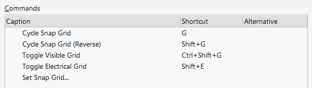
Grids: Commands for configuring and managing grids on the schematic (snap grid, visible grid).
Grids Commands Overview
These commands configure and manage grids on the schematic, including snap grid settings and visible grid display options that help with precise component placement and alignment.
Individual Grid Commands:
Snap Grid Management:
Cycle Snap Grid (G) - Cycles through different snap grid sizes (e.g., 10mil → 5mil → 1mil)
Determines the precision of object placement
Objects automatically snap to grid intersections when placed or moved
Essential for maintaining consistent component spacing
Cycle Snap Grid (Reverse) (Shift+G) - Cycles through snap grid sizes in reverse order
Allows quick access to previously used grid settings
Useful when switching between fine and coarse positioning
Visual Grid Control:
Toggle Visible Grid (Ctrl+Shift+G) - Shows/hides the visual grid display
Grid dots or lines appear on screen as reference
Helps with visual alignment without affecting snap behavior
Can be toggled independently of snap functionality
Toggle Electrical Grid (Shift+E) - Shows/hides the electrical connection grid
Displays grid points where electrical connections can be made
Different from visual grid - focuses on connection points
Critical for proper wire and component pin alignment
Grid Configuration:
Set Snap Grid... - Opens dialog to configure custom snap grid settings
Set specific grid sizes (mils, mm, etc.)
Configure grid display properties
Set up multiple grid levels for different design phases
Key Benefits:
Precision: Ensures accurate component placement and alignment
Consistency: Maintains uniform spacing throughout the design
Efficiency: Quick grid switching for different design tasks
Standards Compliance: Helps meet industry spacing requirements
Typical Workflow:
Use coarse grid (50-100 mil) for initial component placement
Switch to fine grid (10-25 mil) for detailed routing
Use electrical grid to ensure proper pin connections
Toggle visible grid on/off based on visual preference
These grid commands are fundamental for creating professional, well-aligned schematic designs.
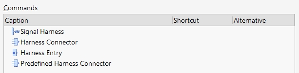
Harness: Tools for creating and managing signal harnesses and their elements (Harness Entries/Connectors).
Harness Commands Overview
These tools create and manage signal harnesses and their associated elements, allowing you to group multiple signals together for cleaner schematic representation and cable/connector design.
Individual Harness Commands:
Core Harness Elements:
Signal Harness - Creates the main harness object that groups multiple signals into a single graphical bundle
Represents multiple wires/signals as one thick line on the schematic
Useful for cable designs, bus connections, and complex multi-wire interfaces
Improves schematic readability by reducing wire clutter
Harness Connector - Places connectors specifically designed for harness connections
Multi-pin connectors that interface with signal harnesses
Automatically handles pin assignments and signal routing
Essential for defining cable entry/exit points
Harness Interface Elements:
Harness Entry - Creates entry points where individual signals connect to or exit from a harness
Allows individual wires to join or leave the harness bundle
Maintains electrical connectivity while providing clean visual representation
Critical for branching signals from main harness runs
Predefined Harness Connector - Places pre-configured harness connectors with standard pinouts
Uses library-defined connector types with predetermined signal assignments
Speeds up design process for common cable/connector combinations
Ensures consistency with industry-standard connector types
Key Benefits:
Visual Clarity: Reduces wire congestion by bundling related signals
Cable Design: Essential for designing wiring harnesses and cable assemblies
Organization: Groups logically related signals (power, data buses, control signals)
Documentation: Provides clear representation of multi-conductor cables
Manufacturing: Generates accurate cable assembly drawings and documentation
Typical Applications:
Automotive Wiring: Engine harnesses, dashboard connections
Industrial Control: Multi-conductor control cables
Computer Systems: Ribbon cables, bus connections
Aerospace: Complex wire bundles and interconnects
These harness tools are essential for designing systems with multiple interconnected cables and complex wiring requirements.
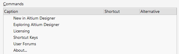
Help: Access to documentation, tutorials, program information.
Let me explain the Help commands in Altium Designer 2025:
Help Commands Overview
These commands provide access to documentation, tutorials, program information, and support resources to help users learn and troubleshoot Altium Designer.
Individual Help Commands:
Getting Started:
New in Altium Designer - Shows information about new features and improvements in the current version
Highlights recent updates and enhancements
Helps users discover new capabilities
Often includes links to detailed feature documentation
Exploring Altium Designer - Provides guided tours and introductory tutorials
Interactive walkthroughs of key features
Step-by-step tutorials for common design tasks
Ideal for new users learning the software
Reference and Support:
Licensing - Opens licensing information and management tools
View current license status and details
Manage license activation and deactivation
Access licensing troubleshooting information
Shortcut Keys - Displays comprehensive list of keyboard shortcuts
Organized by function category
Searchable shortcut reference
Essential for improving workflow efficiency
User Forums - Direct link to Altium's online community forums
Access to user discussions and solutions
Platform for asking questions and sharing knowledge
Community-driven support and tips
Program Information:
About... - Shows program version, build information, and system details
Current software version and build number
License information and registered user details
System configuration and installed components
Useful for technical support and troubleshooting
Key Benefits:
Learning Resources: Comprehensive tutorials and documentation for skill development
Quick Reference: Instant access to shortcuts and feature information
Community Support: Connection to user forums for peer assistance
Technical Information: Version and licensing details for support purposes
These help resources are essential for both new users learning Altium Designer and experienced users looking to optimize their workflow or troubleshoot issues.
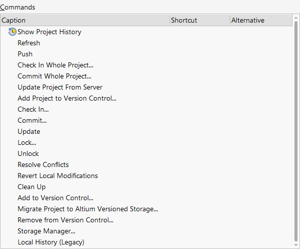
History Version Control: Commands for interacting with version control systems (e.g., Git, SVN), if configured.
Let me explain the History Version Control commands in Altium Designer 2025:
History Version Control Commands Overview
These commands handle interaction with version control systems (Git, SVN, Altium 365) for tracking changes, managing revisions, and enabling team collaboration on design projects.
Individual Version Control Commands:
Project History and Status:
Show Project History - Displays the complete revision history of the project with timestamps, authors, and change descriptions
Refresh - Updates the version control status display to show latest server changes
Local History (Legacy) - Accesses older local history system for backwards compatibility
Basic Version Control Operations:
Check In... - Commits local changes to the version control repository with change comments
Commit... - Similar to Check In, commits changes with detailed change descriptions
Push - Uploads committed changes to remote repository (Git-style workflow)
Update - Downloads latest changes from repository to local working copy
Update Project From Server - Refreshes entire project with server versions
Project-Level Operations:
Check In Whole Project... - Commits all modified files in the project simultaneously
Commit Whole Project... - Commits entire project with single operation and comment
File Locking and Conflict Resolution:
Lock... - Locks files to prevent other users from modifying them
Unlock - Releases file locks to allow other users access
Resolve Conflicts - Opens conflict resolution tools when multiple users modify the same file
Revert Local Modifications - Discards local changes and returns to repository version
Project Management:
Add Project to Version Control... - Initializes version control for a new project
Add to Version Control... - Adds specific files to version control tracking
Remove from Version Control... - Removes files from version control system
Clean Up - Removes temporary version control files and resolves status issues
Advanced Operations:
Migrate Project to Altium Versioned Storage... - Converts projects to use Altium 365 version control
Storage Manager... - Manages version control storage settings and configurations
Key Benefits:
Team Collaboration: Multiple engineers can work on the same project safely
Change Tracking: Complete history of who changed what and when
Backup and Recovery: Automatic backup of all design revisions
Conflict Resolution: Tools to handle simultaneous edits by different users
Release Management: Tag and manage different project versions
These version control tools are essential for professional teams working on complex electronic designs requiring coordination and change management.
Import: Importing data into schematics (e.g., old format files, netlists, data from other CAD systems).

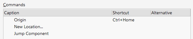
Jump: Navigation commands (e.g., Jump to component, Jump to network, Jump to location mark).
Jump Commands Overview
These navigation commands provide quick ways to move around the schematic by jumping to specific components, networks, locations, or reference points for efficient design navigation.
Individual Jump Commands:
Reference Navigation:
Origin (Ctrl+Home) - Jumps the view to the schematic origin point (0,0 coordinate)
Returns to the default reference point of the schematic
Useful for getting oriented when you're lost in a large design
Provides consistent starting point for navigation
Location Management:
New Location... - Creates a new named location bookmark in the current schematic
Allows you to save specific coordinates or areas for quick return
Useful for marking important circuit sections or reference points
Can be named descriptively (e.g., "Power Supply", "CPU Section")
Component Navigation:
Jump Component - Enables quick navigation to specific components by designator
Type component name (R1, U5, C12, etc.) to jump directly to that component
Essential for large schematics with hundreds of components
Often opens a search dialog or accepts direct component entry
Extended Jump Functionality:
Typical Additional Jump Features (may not be visible in this view):
Jump to Net - Navigate to specific nets by name
Jump to Pin - Navigate to specific component pins
Jump to Location Mark - Jump to previously saved location bookmarks
Cross-reference Navigation - Jump between related schematic elements
Key Benefits:
Efficiency: Rapidly navigate large, complex schematics without scrolling
Precision: Jump directly to specific components or locations
Organization: Use location bookmarks to mark important design areas
Workflow Speed: Eliminate time spent manually searching for components
Typical Usage:
Use Origin to return to schematic center when lost
Create New Location bookmarks for key circuit sections
Use Jump Component to quickly find specific parts during debugging or review
Combine with search functions for comprehensive navigation
These jump commands are essential for efficiently working with large, complex schematic designs where manual navigation would be time-consuming.
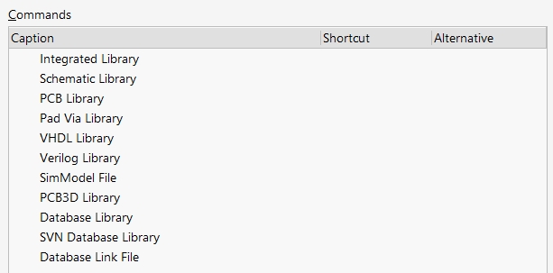
Library: Commands related to schematic symbol libraries (opening, creating, managing, placing components from libraries).
Let me explain the Library commands in Altium Designer 2025:
Library Commands Overview
These commands handle schematic symbol libraries including opening, creating, managing, and working with different types of component libraries for placing components in schematics.
Individual Library Commands:
Core Component Libraries:
Integrated Library - Creates or opens integrated libraries (.IntLib) that combine schematic symbols, PCB footprints, and 3D models in one file
Most comprehensive library format
Contains all component information in single file
Preferred format for complete component definitions
Schematic Library - Creates or opens schematic symbol libraries (.SchLib)
Contains only schematic symbols and electrical properties
Used for creating custom component symbols
Essential for symbol design and editing
PCB Library - Creates or opens PCB footprint libraries (.PcbLib)
Contains physical footprint definitions for PCB layout
Defines pad sizes, shapes, and mechanical dimensions
Required for PCB design phase
Specialized Libraries:
Pad Via Library - Manages pad and via definitions for PCB design
Custom pad shapes and via configurations
Used for specialized PCB requirements
PCB3D Library - Creates 3D model libraries for components
Contains 3D mechanical models for visualization
Essential for mechanical clearance checking
Used in 3D PCB rendering
HDL Libraries:
VHDL Library - Creates VHDL library files for FPGA development
Contains VHDL code modules and functions
Used in embedded/FPGA design workflows
Verilog Library - Creates Verilog library files for digital design
Contains Verilog modules and definitions
Alternative HDL format to VHDL
Simulation and Database:
SimModel File - Creates simulation model libraries
Contains SPICE models and simulation parameters
Essential for circuit simulation and analysis
Database Library - Creates database-linked component libraries
Connects to external component databases
Enables parametric component selection
SVN Database Library - Version-controlled database libraries
Database libraries under SVN version control
For team-managed component libraries
Database Link File - Creates database connection files
Links between Altium and external databases
Manages database connectivity settings
Key Benefits:
Component Management: Organize and maintain component libraries systematically
Design Consistency: Ensure all team members use same component definitions
Integration: Link schematic symbols with PCB footprints and 3D models
Simulation: Include simulation models for circuit analysis
Database Integration: Connect to enterprise component databases
These library commands are fundamental for managing component libraries that form the foundation of professional electronic design workflows.
Location Marks: Tools for placing named marks on the schematic for quick navigation.
Location Marks Commands Overview
These tools allow you to place named marks on the schematic for quick navigation, providing a bookmark system to rapidly move between important areas of your design.
Individual Location Mark Commands:
Numbered Location Marks (1-10):
Location Mark 1 through Location Mark 10 - Creates up to 10 numbered location bookmarks on the schematic
Each mark can be placed at any position on the schematic
Assigned to specific coordinates for precise navigation
Can be named descriptively for easy identification
How Location Marks Work:
Setting Location Marks:
Click on desired location in schematic
Select appropriate numbered location mark command
Mark is saved at current cursor position
Can be renamed with meaningful descriptions
Navigating to Location Marks:
Use corresponding number command to jump to saved location
Instantly centers view on the marked position
Maintains zoom level for consistent viewing
Key Benefits:
Quick Navigation: Instantly jump between important circuit sections
Design Organization: Mark key areas like power supplies, interfaces, critical paths
Review Efficiency: Quickly move between areas during design reviews
Troubleshooting: Mark problem areas for easy return during debugging
Typical Usage Examples:
Common Bookmark Uses:
Mark 1: Power supply section
Mark 2: Microcontroller/CPU area
Mark 3: I/O connectors
Mark 4: Clock generation
Mark 5: Analog front-end
Mark 6: Communication interfaces
Mark 7: Test points
Mark 8: Critical timing paths
Mark 9: Problem areas under review
Mark 10: Reference designs or notes
Workflow Integration:
Set location marks during initial design review
Use marks to quickly navigate during component placement
Update marks as design evolves
Share mark locations with team members for collaborative reviews
This bookmark system is essential for efficiently navigating large, complex schematic designs with multiple functional blocks.
Managed Project: Commands related to managed projects on Altium 365 servers or Concord Pro (e.g., check-in, check-out, synchronization).
Managed Project Commands Overview
These commands handle managed projects on Altium 365 servers or Concord Pro systems, providing enterprise-level project management with check-in, check-out, synchronization, and collaborative features.
Individual Managed Project Commands:
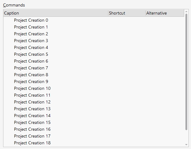
Project Creation Templates (0-18+):
Project Creation 0 through Project Creation 18 - Pre-configured project templates for different types of managed projects
Each number represents a different project template or workflow
Templates may include different design methodologies, component libraries, or design rules
Standardized starting points for consistent project structure across teams
Key Features of Managed Projects:
Server-Based Management:
Projects stored on Altium 365 cloud servers or on-premise Concord Pro servers
Centralized project storage and access control
Automatic backup and version history
Collaboration Features:
Multi-user access with role-based permissions
Concurrent editing with conflict resolution
Real-time synchronization between team members
Comment and review systems for design collaboration
Project Lifecycle Management:
Standardized project templates ensure consistency
Workflow enforcement for design processes
Release management and approval workflows
Integration with company design standards
Benefits of Managed Projects:
Team Collaboration: Multiple engineers can work on the same project simultaneously
Standardization: Consistent project structure across all designs
Version Control: Automatic versioning and change tracking
Access Control: Secure access with user permissions and roles
Integration: Seamless integration with enterprise systems and workflows
Typical Usage:
Select appropriate Project Creation template based on design type
Template creates standardized project structure with:
Pre-configured libraries
Standard design rules
Company-specific settings
Workflow definitions
Team members can then collaborate on the managed project with proper version control
These managed project templates are essential for organizations that need standardized, collaborative design workflows with enterprise-level project management capabilities.
Mixed-Signal Simulation: Commands for setting up and running mixed analog-digital circuit simulations (if simulator tools are active/licensed).
Mixed-Signal Simulation Commands Overview
These commands handle setup and execution of mixed analog-digital circuit simulations, enabling you to simulate circuits that contain both analog components and digital logic using integrated simulation tools.
Individual Mixed-Signal Simulation Commands:
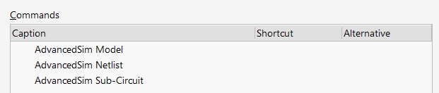
Simulation Model Management:
AdvancedSim Model - Creates or manages simulation models for components
Defines SPICE models for analog components (resistors, capacitors, transistors, op-amps)
Sets up behavioral models for digital components
Links schematic symbols to their corresponding simulation models
Essential for accurate circuit behavior prediction
Netlist Generation:
AdvancedSim Netlist - Generates netlists specifically formatted for mixed-signal simulation
Extracts circuit connectivity from the schematic
Combines analog SPICE netlist with digital logic descriptions
Handles interface between analog and digital domains
Prepares circuit description for simulation engine
Hierarchical Simulation:
AdvancedSim Sub-Circuit - Creates sub-circuit definitions for hierarchical simulation
Encapsulates complex circuit blocks as reusable sub-circuits
Enables simulation of large designs by breaking them into manageable blocks
Supports hierarchical design methodology in simulation
Improves simulation performance and organization
Key Simulation Capabilities:
Mixed-Signal Analysis:
Simultaneous analog and digital simulation
Accurate modeling of analog-digital interfaces
Support for various analysis types (DC, AC, transient, noise)
Real-time waveform viewing and analysis
Model Integration:
SPICE models for analog components
Digital behavioral models
Vendor-provided models
Custom user-defined models
Simulation Types:
DC operating point analysis
AC small-signal analysis
Transient (time-domain) analysis
Noise analysis
Monte Carlo analysis
Prerequisites:
Requires active/licensed simulator tools in Altium Designer
Components must have appropriate simulation models
Mixed-signal simulation license may be required
These simulation commands enable verification of circuit behavior before physical prototyping, crucial for complex mixed-signal designs in applications like data converters, power management, and sensor interfaces.
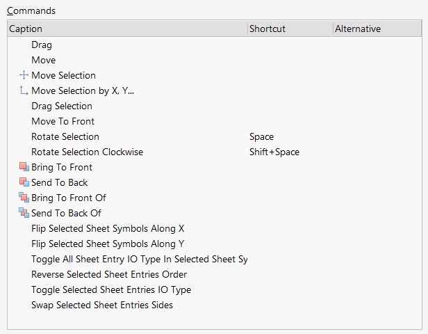
Move: Commands for moving selected objects.
Move Commands Overview
These commands provide various methods for moving, positioning, rotating, and manipulating selected objects in the schematic, including precise positioning and layer management.
Individual Move Commands:
Basic Movement:
Drag - Interactive dragging of objects with mouse cursor
Move - Activates move mode for selected objects
Move Selection - Moves currently selected objects to a new position
Move Selection by X, Y... - Moves objects by specific coordinate distances
Allows precise positioning with exact X,Y offset values
Useful for alignment and consistent spacing
Drag Selection - Drag mode specifically for selected objects
Rotation Commands:
Rotate Selection (Space) - Rotates selected objects counterclockwise in 90° increments
Rotate Selection Clockwise (Shift+Space) - Rotates selected objects clockwise in 90° increments
Layer/Z-Order Management:
Move To Front - Brings selected objects to the front of the drawing order
Bring To Front - Similar to Move To Front, ensures objects appear on top
Send To Back - Sends selected objects to the back of the drawing order
Bring To Front Of - Brings objects in front of a specific reference object
Send To Back Of - Sends objects behind a specific reference object
Hierarchical Sheet Manipulation:
Flip Selected Sheet Symbols Along X - Mirrors sheet symbols horizontally
Flip Selected Sheet Symbols Along Y - Mirrors sheet symbols vertically
Toggle All Sheet Entry IO Type In Selected Sheet Sy - Changes I/O direction for all sheet entries
Reverse Selected Sheet Entries Order - Reverses the order of sheet entry pins
Toggle Selected Sheet Entries IO Type - Changes input/output direction of selected entries
Swap Selected Sheet Entries Sides - Moves sheet entries to opposite sides of the symbol
Key Benefits:
Precision: Exact coordinate-based movement for precise placement
Efficiency: Quick rotation and flipping for component orientation
Organization: Layer management for controlling object overlap
Hierarchical Design: Specialized tools for managing sheet symbols and their interfaces
Typical Workflow:
Select objects to move
Use Move Selection for basic repositioning
Use Rotate Selection (Space) to orient components properly
Use Move Selection by X, Y for precise alignment
Manage drawing order with Bring To Front/Send To Back commands
These move commands are essential for organizing and positioning elements in professional schematic designs.
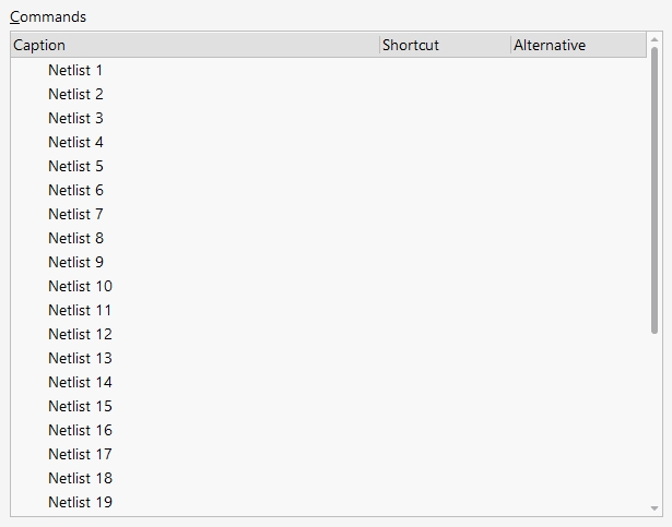
Netlist For Document: Generating a netlist for the current schematic document.
Netlist For Document Commands Overview
These commands generate netlists for the current schematic document, creating connectivity information in various formats for different target applications and tools.
Individual Netlist Commands:
Numbered Netlist Formats (1-19+):
Netlist 1 through Netlist 19 - Different netlist output formats and configurations
Each number represents a specific netlist format or target application
Pre-configured netlist generators for different purposes
May include formats for various PCB layout tools, simulators, or analysis software
Common Netlist Types and Applications:
PCB Layout Transfer:
PCB netlist formats for transferring schematic connectivity to PCB layout tools
Altium Designer native format for seamless schematic-to-PCB workflow
Third-party PCB tool formats (Cadence, Mentor Graphics, etc.)
Simulation Netlists:
SPICE netlist formats for circuit simulation
Mixed-signal simulation netlists
Digital logic simulation formats
Manufacturing and Assembly:
Pick-and-place machine formats
Bill of Materials (BOM) generation
Assembly drawing netlists
Analysis Tools:
Signal integrity analysis formats
Thermal analysis netlists
EMC/EMI analysis formats
Key Netlist Information:
Connectivity Data:
Component-to-component connections
Net names and signal routing
Component reference designators
Pin assignments and connections
Component Information:
Component values and parameters
Package information
Placement coordinates (if applicable)
Component attributes and properties
Typical Usage:
Complete schematic design and annotation
Select appropriate netlist format based on target application
Configure netlist parameters (if needed)
Generate netlist for export to other tools
Verify netlist accuracy before transfer
Workflow Integration:
Schematic → PCB: Generate PCB netlist for layout design
Schematic → Simulation: Create SPICE netlist for circuit analysis
Schematic → Manufacturing: Generate assembly and BOM data
These netlist commands are essential for transferring design information from the schematic environment to downstream tools in the electronic design workflow.
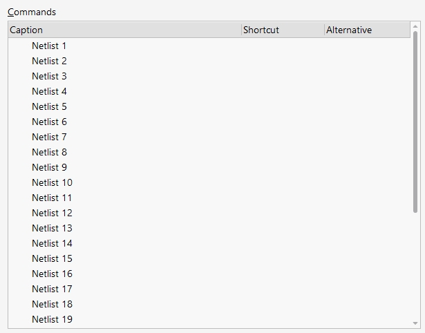
Netlist For Project: Generating a netlist for the entire project.
Let me explain the Netlist For Project commands in Altium Designer 2025:
Netlist For Project Commands Overview
These commands generate netlists for the entire project, creating comprehensive connectivity information across all schematic sheets and hierarchical levels, rather than just the current document.
Individual Netlist Commands:
Numbered Netlist Formats (1-19+):
Netlist 1 through Netlist 19 - Different project-wide netlist output formats and configurations
Each number represents a specific netlist format targeting different applications
Processes all schematic sheets in the project simultaneously
Resolves hierarchical connections across multiple sheets
Pre-configured formats for various downstream tools
Key Differences from Document Netlists:
Project-Wide Scope:
Includes all schematic sheets in the project
Resolves hierarchical sheet connections
Processes multi-sheet designs as single system
Handles cross-sheet connectivity automatically
Hierarchical Design Support:
Connects parent and child sheet symbols
Resolves port connections between hierarchy levels
Maintains signal continuity across sheet boundaries
Flattens hierarchical design into flat netlist
Common Project Netlist Applications:
Complete System Transfer:
Full project PCB netlist for complex multi-board systems
System-level simulation netlists
Complete Bill of Materials (BOM) generation
Comprehensive connectivity verification
Manufacturing Documentation:
Complete assembly instructions across all boards
System-level test and verification netlists
Full project documentation packages
Analysis and Verification:
System-wide signal integrity analysis
Complete electrical rule checking
Cross-sheet connectivity verification
Project-wide component usage reports
Typical Project Workflow:
Complete all schematic sheets in project
Annotate components across entire project
Verify hierarchical connections
Select appropriate project netlist format
Generate comprehensive project netlist
Transfer to PCB layout or other downstream tools
Key Benefits:
Completeness: Captures entire system connectivity
Hierarchy Resolution: Automatically handles complex hierarchical designs
System Integration: Ensures all project elements are included
Multi-Sheet Support: Essential for large, complex designs
These project-level netlist commands are crucial for multi-sheet designs and hierarchical projects where you need complete system-level connectivity information.
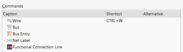
Nets: Commands for managing networks (highlighting, navigation, network properties).
Let me explain the Nets commands in Altium Designer 2025:
Nets Commands Overview
These commands manage networks (electrical connections) in schematics, including highlighting, navigation, and network properties. They're essential for creating and managing electrical connectivity between components.
Individual Nets Commands:
Basic Connectivity:
Wire (Ctrl+W) - Places individual wires to connect component pins
Creates point-to-point electrical connections
Most fundamental tool for schematic connectivity
Automatically creates electrical nodes at junctions
Essential for all circuit connections
Bus Systems:
Bus - Places multi-wire buses for grouped signal connections
Represents multiple related signals as single thick line
Used for data buses, address buses, control signal groups
Reduces visual clutter for multi-bit connections
Common in digital designs (8-bit data bus, 16-bit address bus)
Bus Entry - Creates connection points where individual wires connect to buses
Allows individual signals to join or leave bus structures
Maintains electrical connectivity while providing clean visual representation
Essential for accessing individual signals from bus groups
Labeling and Documentation:
Net Label - Places text labels to identify and name networks
Names electrical connections for clarity and documentation
Enables connections across schematic sheets (nets with same name connect)
Critical for multi-sheet designs and hierarchical schematics
Improves readability and troubleshooting
Advanced Connectivity:
Functional Connection Line - Creates logical connections without physical wires
Shows functional relationships between circuit blocks
Used for control signals, enable lines, or conceptual connections
Helps document circuit operation without cluttering the schematic
Useful in block diagrams and high-level representations
Key Benefits:
Electrical Connectivity: Establishes all electrical connections between components
Organization: Bus systems group related signals for cleaner schematics
Documentation: Net labels provide clear signal identification
Multi-Sheet Design: Named nets connect across multiple schematic pages
Visual Clarity: Different connection types for different purposes
Typical Workflow:
Use Wire (Ctrl+W) for basic component-to-component connections
Use Bus and Bus Entry for grouped digital signals
Add Net Labels to identify important signals and enable cross-sheet connections
Use Functional Connection Line for logical relationships
These net commands form the foundation of schematic connectivity and are used constantly during circuit design.
New: Similar to "Add New to Project," but may be more general or focused on creating new separate files.
New Commands Overview
These commands create new separate files and documents for various aspects of electronic design, from projects and schematics to manufacturing outputs and libraries.
Individual New Commands:
Project and System Level:
Project... - Creates a new Altium Designer project file
Multi-board Schematic - Creates multi-board system schematic
Multi-board Assembly - Creates assembly documentation for multi-board systems
Design Project Group - Creates a group of related design projects
Electronics System Design Document - Creates system-level design documentation
Schematic Documents:
Schematic - Creates a new schematic sheet document
Finite State Machine Document - Creates FSM diagrams for digital logic design
PCB Design:
PCB - Creates a new PCB layout document
PCB3D - Creates 3D mechanical PCB document
Wiring and Harness:
Harness Wiring Diagram - Creates cable and harness wiring diagrams
Harness Layout Drawing - Creates physical harness layout documentation
Manufacturing and Assembly:
ActiveBOM - Creates intelligent Bill of Materials document
CAM Document - Creates Computer-Aided Manufacturing files
Output Job File - Creates automated output generation configurations
Mechanical Design:
Draftsman Document - Creates mechanical drawings and documentation
Component and Library Management:
Component... - Creates new component definitions
Reuse Block... - Creates reusable circuit blocks
Library... - Creates various types of component libraries
Configuration and Management:
Files Panel (Ctrl+N) - Opens file management panel
Components Synchronization Configuration - Sets up component library synchronization
Custom Parts Provider Synchronization Configuration - Configures custom parts database sync
Documentation:
Text Document - Creates general text documentation files
Key Categories:
Design Documents: Core schematic and PCB files for circuit design
Manufacturing: Files needed for PCB fabrication and assembly
Documentation: Technical drawings, BOMs, and project documentation
Libraries: Component libraries and reusable design blocks
Project Management: Project organization and configuration files
System Design: Multi-board and system-level design documents
Typical Workflow:
Start with Project... to create new project container
Add Schematic sheets for circuit design
Create PCB document for layout design
Add Output Job File for manufacturing outputs
Create Library files for custom components
These New commands provide the foundation for creating all types of documents needed in professional electronic design projects.
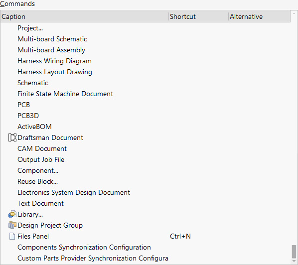
Panels: Commands for displaying/hiding various interface panels (Projects, Libraries, Inspector, Messages, etc.).
Panels Commands Overview These commands control the display and hiding of various interface panels that provide different functionality and information in Altium Designer's workspace, such as Projects, Libraries, Inspector, Messages, and other tool panels. Individual Panel Commands: Toggle Panel Commands (1-19+):Toggle Panel 1 Category 1 through Toggle Panel 19 Category 1 - Show/hide different interface panels
Each numbered panel represents a specific functional panel in the interface
"Category 1" indicates these are core workspace panels
Toggle functionality allows quick show/hide of panels to optimize workspace
Common Panel Types in Altium Designer:
Project Management:
Projects Panel - Shows project structure, files, and hierarchy
Storage Manager Panel - Manages version control and file storage
History Panel - Displays project revision history
Component and Library Management:
Libraries Panel - Access to component libraries and parts
Components Panel - Browse and search components
Manufacturer Part Search Panel - Find real-world component parts
Design Analysis:
Inspector Panel - Shows properties of selected objects
Messages Panel - Displays errors, warnings, and compilation messages
Navigator Panel - Hierarchical design navigation
List Panel - Tabular view of design objects
Simulation and Analysis:
Workspace Panel - Simulation controls and settings
SPICE Analysis Panel - Circuit simulation tools
Signal Integrity Panel - High-speed design analysis
Manufacturing and Output:
ActiveBOM Panel - Bill of Materials management
Output Job Panel - Manufacturing output configuration
Key Benefits:
Workspace Optimization: Show only panels needed for current task
Efficiency: Quick access to frequently used tools and information
Customization: Arrange workspace based on personal workflow
Context Sensitivity: Different panels for different design phases
Typical Usage:
Use Projects Panel for file management and navigation
Toggle Libraries Panel when placing components
Show Inspector Panel when editing object properties
Display Messages Panel during compilation and error checking
Hide unused panels to maximize schematic viewing area
These panel toggle commands allow you to customize the Altium Designer interface for optimal productivity based on your current design task.
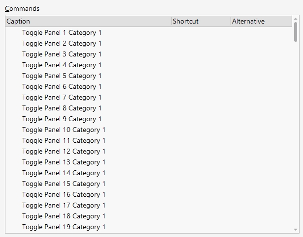
Place: Main category for placing electrical objects: wires, buses, ports, components, power ports, No ERC markers, directives, etc.
Place Commands Overview
This is the main category for placing electrical objects, components, and schematic elements including wires, buses, ports, components, power connections, and various schematic symbols.
Individual Place Commands:
Basic Connectivity:
Wire (Ctrl+W) - Places wires for electrical connections between components
Bus - Places multi-wire buses for grouped signals
Bus Joiner - Connects multiple buses together
Bus Entry - Creates connection points between individual wires and buses
Net Label - Places text labels to name and identify networks
Components and Parts:
Part... - Places components from libraries onto the schematic
Power Port - Places power supply connection symbols (VCC, GND, etc.)
Hierarchical Design:
Port - Places hierarchical connection ports for multi-sheet designs
Off Sheet Connector - Creates connections that continue on other schematic sheets
Sheet Symbol - Places hierarchical sheet symbols for modular design
Sheet Entry - Creates connection points on sheet symbols
Device Sheet Symbol - Places device-specific sheet symbols
Reusable Design Elements:
Reuse Block... - Places pre-designed circuit blocks
C Code Symbol - Places embedded code symbols
Add C Code Entry - Adds entries to code symbols
Harness and Cable Design:
Harness Wire (Shift+W) - Places harness wires for cable design
Harness Cable - Places cable representations in harness designs
Harness Bundle (Shift+B) - Creates bundled wire groups
Harness Covering - Adds protective covering to harness designs
Connection Management:
Splice - Creates wire splice connections
Tap - Places tap connections on existing wires
Connection Point - Places explicit connection points
Twist - Shows twisted pair connections
Wire Break - Creates breaks in wire connections
Shielding and EMI:
Shield - Places shielding symbols for EMI protection
Shield with Connection - Places grounded shield symbols
Text and Annotation:
Text String - Places text annotations and labels
Text Frame - Creates bordered text areas
Note - Places design notes and comments
Comment... (Ctrl+Alt+C) - Adds design comments and annotations
Special Elements:
Layout Label - Places labels for PCB layout reference
No Connect - Places "No Connect" symbols on unused pins
Key Categories:
Electrical Connectivity: Wires, buses, and connection elements
Component Placement: Parts, power ports, and symbols
Hierarchical Design: Multi-sheet design elements
Documentation: Text, labels, and annotations
Specialized Design: Harness, shielding, and advanced features
Typical Workflow:
Use Part... to place components from libraries
Use Wire (Ctrl+W) to connect component pins
Add Power Port for power connections
Use Net Label to name important signals
Add Text String and Comment for documentation
These Place commands are the primary tools for building schematic designs and form the core of the schematic entry workflow.
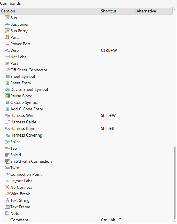
Place Models: Placing models for simulation or possibly linking with footprints (although footprint placement usually occurs in PCB). In schematics, this likely relates to simulation models.
Place Models Commands Overview
These commands are for placing models for simulation or linking with footprints. In schematics, this primarily relates to simulation models that define how components behave during circuit analysis.
Typical Place Models Functions:
Simulation Model Placement:
SPICE Models - Place behavioral models for analog simulation
Defines electrical characteristics of components
Used for transient, AC, and DC analysis
Essential for accurate circuit simulation
Digital Models - Place logic models for digital components
Defines timing characteristics and logic behavior
Used for digital simulation and timing analysis
Important for mixed-signal designs
Model Linking:
Footprint Association - Links schematic symbols to PCB footprints
Connects logical schematic representation to physical PCB layout
Usually handled automatically through integrated libraries
Critical for schematic-to-PCB transfer
3D Model Links - Associates 3D mechanical models with components
Used for 3D visualization and mechanical clearance checking
Helps with enclosure design and component placement
Key Applications:
Circuit Simulation:
Analog circuit analysis using SPICE models
Digital timing simulation
Mixed-signal system verification
Parameter sweeps and optimization
Design Verification:
Pre-prototype circuit validation
Performance prediction
Design rule verification
Signal integrity analysis
Typical Workflow:
Place components with associated simulation models
Run circuit simulations to verify design performance
Iterate design based on simulation results
Link to appropriate PCB footprints for layout
Note: The specific commands in this category may be context-dependent or require simulation tools to be active/licensed. The exact available commands would depend on your Altium Designer installation and enabled simulation capabilities.
This functionality bridges the gap between schematic design and both simulation analysis and physical implementation.
Place Probes: Placing probes for simulation (for measuring voltage, current, etc.).
Let me explain the Place Probes commands in Altium Designer 2025:
Place Probes Commands Overview
These commands place simulation probes on the schematic for measuring electrical parameters (voltage, current, power, etc.) during circuit simulation and analysis.
Individual Probe Commands:
Voltage Measurement:
Voltage - Places voltage probes to measure voltage at specific nodes
Measures voltage relative to ground reference
Essential for monitoring signal levels and DC operating points
Used in transient, AC, and DC analysis
Shows voltage waveforms in simulation results
Voltage Diff - Places differential voltage probes
Measures voltage difference between two points
Critical for differential signal analysis
Used for measuring voltage drops across components
Important for op-amp and differential circuit analysis
Current Measurement:
Current - Places current probes to measure current flow through branches
Measures current flowing through wires or component leads
Essential for power analysis and circuit verification
Used to verify current ratings and component stress
Shows current waveforms during simulation
Power Analysis:
Power - Places power probes to measure power consumption or dissipation
Calculates instantaneous and average power
Critical for thermal analysis and battery life estimation
Used to optimize power efficiency
Important for power management circuit design
Key Applications:
Circuit Verification:
Verify operating voltages meet specifications
Check current levels within component ratings
Monitor power consumption for efficiency analysis
Validate signal integrity and timing
Design Optimization:
Identify power-hungry circuit sections
Optimize component values for desired performance
Minimize power consumption in battery-powered designs
Balance performance vs. power trade-offs
Troubleshooting:
Identify unexpected voltage levels
Find excessive current draw
Locate power dissipation hotspots
Debug circuit malfunctions
Typical Workflow:
Place probes at critical circuit nodes during schematic design
Run simulation analysis (transient, AC, DC)
View probe results in waveform viewer
Analyze performance and optimize design
Iterate design based on measurement results
Simulation Types:
DC Analysis: Steady-state voltage and current levels
Transient Analysis: Time-domain waveforms and power consumption
AC Analysis: Frequency response and impedance analysis
These probe commands are essential for thorough circuit simulation and verification before physical prototyping.
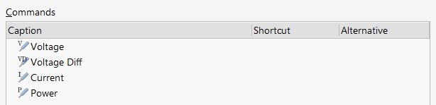
Place Sources: Placing voltage/current sources for simulation.
Place Sources Commands Overview
These commands place voltage and current sources specifically for circuit simulation, providing the stimulus signals needed to analyze circuit behavior during simulation runs.
Individual Source Commands:
Voltage Sources:
Voltage Source - Places voltage sources for simulation stimulus
DC voltage sources for bias and operating point analysis
AC voltage sources for frequency response analysis
Transient voltage sources for time-domain analysis
Pulse, sine, square wave, and custom waveform generators
Essential for powering circuits during simulation
Current Sources:
Current Source - Places current sources for simulation
DC current sources for bias current injection
AC current sources for small-signal analysis
Transient current sources for dynamic analysis
Used for current-mode circuit analysis
Important for testing current-driven circuits
Key Source Types and Parameters:
DC Sources:
Constant voltage/current levels
Used for operating point and bias analysis
Sets steady-state conditions for circuit operation
AC Sources:
Sinusoidal signals for frequency response
Magnitude and phase specifications
Used for small-signal AC analysis
Critical for filter and amplifier characterization
Transient Sources:
Time-varying waveforms (pulse, ramp, exponential)
Custom piecewise linear waveforms
Used for transient and switching analysis
Essential for digital and power circuit simulation
Simulation Applications:
Circuit Stimulation:
Provide power supply voltages for circuit operation
Generate test signals for circuit response analysis
Create stimulus patterns for digital logic verification
Supply bias currents for analog circuit operation
Analysis Types:
DC Analysis: Steady-state voltage and current sources
AC Analysis: Small-signal frequency domain stimulus
Transient Analysis: Time-domain waveform generation
Parametric Sweeps: Variable source parameters for optimization
Typical Usage:
Place Voltage Source for power supply connections (VDD, VCC)
Add Voltage Source for input signal generation
Use Current Source for bias current injection
Configure source parameters (amplitude, frequency, waveform type)
Run simulation analysis to observe circuit response
These source commands are fundamental for creating realistic simulation environments that accurately model how circuits will behave with actual power supplies and input signals.
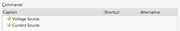
Port Cross Reference: Tools for generating or managing cross-references for ports between hierarchical sheets.
Let me explain the Port Cross Reference commands in Altium Designer 2025:
Port Cross Reference Commands Overview
These tools generate or manage cross-references for ports between hierarchical sheets, providing documentation and navigation aids for complex multi-sheet designs with hierarchical structure.
Individual Port Cross Reference Commands:
Project Management:
Add To Project - Adds port cross-reference documentation to the current project
Creates cross-reference reports showing port connections across hierarchy levels
Generates tabular documentation of parent-child sheet port relationships
Adds cross-reference documents to project for easy access and updates
Remove From Project - Removes port cross-reference documentation from the project
Removes previously generated cross-reference reports
Cleans up project structure when cross-reference docs are no longer needed
Maintains project organization by removing outdated documentation
Key Functions of Port Cross References:
Hierarchical Design Documentation:
Shows how ports on parent sheets connect to child sheet entries
Documents signal flow through hierarchical design levels
Provides tabular view of all port connections in the project
Essential for understanding complex multi-sheet designs
Design Navigation:
Enables quick navigation between related ports across sheets
Provides clickable links to jump between hierarchical levels
Shows port usage and connectivity throughout the project
Helps trace signals through multiple design hierarchy levels
Design Verification:
Verifies that all hierarchical connections are properly made
Identifies unconnected or mismatched ports
Ensures signal integrity across hierarchical boundaries
Supports design review and documentation processes
Typical Applications:
Complex System Design: Multi-board systems with hierarchical organization
Team Collaboration: Documentation for team members working on different sheets
Design Review: Comprehensive port connectivity verification
Project Documentation: Professional documentation packages for design handoff
Workflow:
Complete hierarchical design with parent and child sheets
Use Add To Project to generate comprehensive port cross-reference
Review cross-reference documentation for connectivity verification
Use cross-reference for navigation during design modifications
Update cross-reference as design evolves
These tools are essential for managing and documenting complex hierarchical designs where tracking port relationships across multiple sheets is critical.
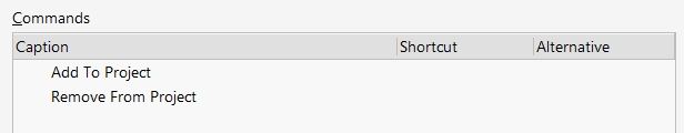
Power Ports: Commands for placing power port symbols (VCC, GND, etc.).
Let me explain the Power Ports commands in Altium Designer 2025:
Power Ports Commands Overview
These commands place power port symbols (VCC, GND, etc.) to establish power connections in schematics. Power ports automatically connect all instances with the same name across the entire project.
Individual Power Port Commands:
Common Power Supplies:
Place GND power port - Places ground connection symbols
Most common power port for 0V reference
Automatically connects all GND symbols throughout the project
Essential for establishing circuit reference potential
Place VCC power port - Places positive power supply connections
Standard symbol for main positive supply voltage
Typically +5V, +3.3V, or other main supply voltages
Connects all VCC instances across all schematic sheets
Specific Voltage Levels:
Place +12 power port - Places +12V power supply connections
Place +5 power port - Places +5V power supply connections
Place -5 power port - Places -5V (negative) power supply connections
Pre-labeled for specific common voltage levels
Reduces labeling errors and ensures consistency
Useful for designs with multiple supply voltages
Different Visual Styles:
Place Arrow style power port - Power port with arrow symbol
Place Wave style power port - Power port with wave/AC symbol
Place Bar style power port - Power port with horizontal bar
Place Circle style power port - Power port with circular symbol
Different visual representations for same electrical function
Choose based on company standards or personal preference
All function identically - only appearance differs
Specialized Ground Types:
Place Signal Ground power port - Dedicated signal ground reference
Used to distinguish signal ground from power ground
Important in mixed-signal designs for noise isolation
Helps maintain clean signal references
Place Earth power port - Earth/chassis ground connection
Represents physical earth ground or chassis connection
Different from circuit ground (GND)
Used for safety and EMI considerations
Key Benefits:
Global Connectivity: All power ports with same name automatically connect
Clean Schematics: Eliminates need for power wires across entire schematic
Multiple Supplies: Easy management of different voltage levels
Professional Appearance: Standard symbols recognized industry-wide
Typical Usage:
Place GND ports near all components requiring ground connection
Use VCC or specific voltage ports (+5, +12) for power supplies
Connect component power pins directly to nearby power ports
Use different ground types (Signal Ground, Earth) when needed for design separation
These power port commands are fundamental for creating clean, professional schematics with proper power distribution.
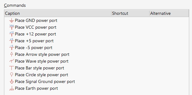
Project: Project-level operations (Compilation, Build, Project Options, Show Differences).
Let me explain the Project commands in Altium Designer 2025: Project Commands Overview These are project-level operations for compilation, build processes, project management, version control, configuration management, and various project utilities. Individual Project Commands: Project Availability: Make Available Online... - Publishes project to Altium 365 cloud platform Make Available on Server... - Makes project available on company server Compilation and Build: Compile Current Project - Compiles all documents in the current project Halt Compilation - Stops ongoing compilation process Cross Probe Next Message (Ctrl+Shift+F3) - Navigates to next compilation error/warning Cross Probe Previous Message (Ctrl+Shift+F4) - Navigates to previous compilation message Project Management:Add Existing to Project... - Adds existing files to the current project
Remove from Project... - Removes selected files from project
Project Documents... (Ctrl+Alt+O, Ctrl+F12) - Opens project documents manager
Close Project Documents - Closes all open project documents
Close Project - Closes the entire project
Server Integration:
Link Project To Server... - Links project to version control server
Release Project To Server... - Releases project version to server
Discard Project Local Changes - Reverts local modifications to server version
Analysis and Comparison:
Show Differences... - Compares project versions for changes
Show Physical Differences... - Shows physical/layout differences between versions
Component Links... - Manages component library links and references
Variants... - Manages project variants and configurations
Project Packaging and Distribution:
Project Packager... - Packages project with all dependencies for sharing
Export Configuration... - Exports project configuration settings
Project Releaser... - Creates release packages for manufacturing
Project Order... - Manages project ordering and priorities
Configuration Management:
Configuration Manager... (appears twice) - Manages project configurations and build settings
FPGA Workspace Map... - Maps FPGA workspace configurations
Import Changes From FPGA Project... - Imports changes from FPGA development tools
Utilities:
Assembly Assistant - Helps with PCB assembly documentation
Show in Explorer - Opens project location in Windows Explorer
Show in Web Browser - Opens project in web browser (for cloud projects)
Share... - Shares project with team members or external parties
Project Settings:
Project Options... - Configures project-wide settings and preferences
Document Options... - Sets document-specific options and parameters
Key Categories:
Build Management: Compilation, error checking, and build processes
Version Control: Server integration, change tracking, and collaboration
Configuration: Project variants, settings, and build configurations
Distribution: Packaging, releasing, and sharing projects
Analysis: Comparison tools and component management
These project commands provide comprehensive project lifecycle management from initial development through manufacturing release.
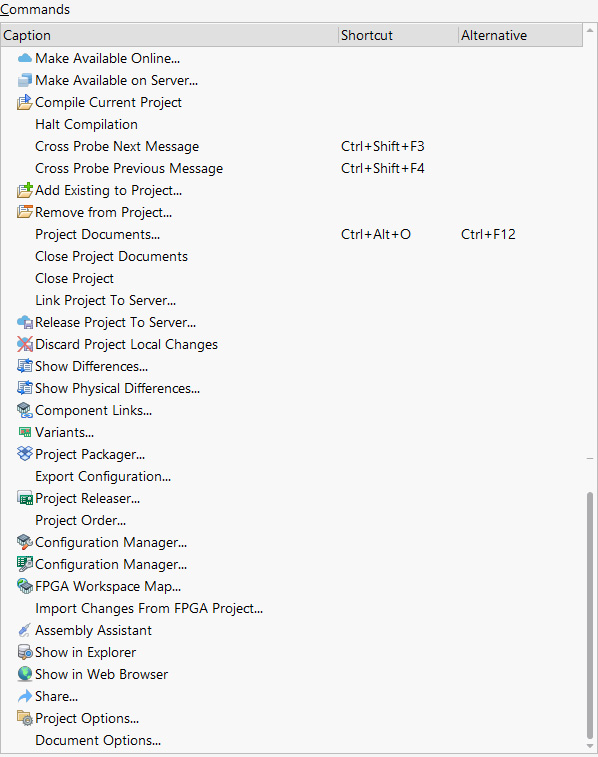
Project Activities: Likely related to managed projects, change tracking, or tasks.
Project Activities Commands Overview
These commands are related to managed projects, change tracking, and task management, providing workflow support for enterprise-level project management and team collaboration.
Individual Project Activity Commands:
Numbered Activity Commands (0-18+):
Project Activity 0 through Project Activity 18 - Different types of project activities or workflow steps
Each number represents a specific project activity or task type
Pre-configured workflow steps for managed project environments
Context-dependent activities based on project type and organization settings
May represent different phases of the design process
Typical Project Activity Types:
Design Phase Activities:
Schematic capture milestones
Design review checkpoints
Component selection and approval
Simulation and verification tasks
Design rule checking completion
Collaboration Activities:
Team member assignments
Review and approval workflows
Change request processing
Design iteration tracking
Documentation updates
Release Management:
Design freeze points
Manufacturing readiness checks
Quality assurance milestones
Release approval processes
Version control checkpoints
Key Functions:
Workflow Management:
Structured design process enforcement
Milestone tracking and reporting
Task assignment and completion tracking
Progress monitoring across team members
Change Control:
Controlled design modifications
Change request documentation
Impact analysis and approval
Audit trail maintenance
Quality Assurance:
Design review requirements
Verification and validation steps
Compliance checking
Documentation completeness
Enterprise Integration:
Managed Project Support:
Integration with Altium 365 workflows
Enterprise design process compliance
Automated workflow enforcement
Project status reporting
Team Collaboration:
Multi-user project coordination
Role-based activity assignments
Communication and notification systems
Progress visibility across teams
Typical Usage:
Activities are typically configured by project administrators
Team members complete assigned activities based on their role
System tracks progress and enforces workflow requirements
Management can monitor project status through activity completion
These Project Activity commands enable structured, enterprise-level project management with defined workflows, milestones, and team coordination capabilities.
Project Releaser: Commands for the project release process (generation of production files, packaging).
Let me explain the Project Releaser commands in Altium Designer 2025:
Project Releaser Commands Overview
These commands handle the project release process, including generation of production files, packaging, and creating deliverables for manufacturing, assembly, and project handoff.
Individual Project Release Commands:
Numbered Release Configurations (0-18+):
Project Release 0 through Project Release 18 - Different release configurations or output packages
Each number represents a specific release configuration or output job
Pre-configured release packages for different purposes or manufacturing stages
Customizable release workflows for different project types or customers
Typical Release Package Contents:
Manufacturing Files:
Gerber files for PCB fabrication
Excellon drill files for hole drilling
Pick and place files for automated assembly
Bill of Materials (BOM) for component procurement
Assembly drawings and fabrication notes
Documentation Packages:
Schematic PDF outputs
PCB assembly drawings
Component placement reports
Test and inspection documentation
User manuals and technical specifications
Quality Assurance:
Design rule check reports
Electrical rule check results
Component compliance documentation
Test procedures and specifications
Certification and approval documentation
Common Release Types:
Prototype Release:
Files needed for prototype PCB fabrication
Basic assembly documentation
Initial testing procedures
Production Release:
Complete manufacturing package
Detailed assembly instructions
Quality control specifications
Supplier qualification requirements
Customer Release:
Documentation packages for customer delivery
User guides and technical manuals
Support documentation and contact information
Archive Release:
Complete project archive for long-term storage
All source files and generated outputs
Project history and change documentation
Key Benefits:
Automated Output Generation: Consistent, repeatable release packages
Quality Control: Ensures all required files are included in releases
Version Management: Tracks different release versions and configurations
Manufacturing Ready: Generates industry-standard manufacturing files
Typical Workflow:
Configure release packages for different purposes (prototype, production, etc.)
Select appropriate Project Release number based on target use
System automatically generates all required files and documentation
Package is created ready for delivery to manufacturers or customers
Release is documented and archived for future reference
These release commands streamline the transition from design completion to manufacturing and ensure all necessary files and documentation are properly generated and packaged.
Recall: Possibly restoring previously saved views or settings.
Let me explain the Recall commands in Altium Designer 2025:
Recall Commands Overview
These commands restore previously saved views, zoom levels, or settings, providing a quick way to return to specific schematic views or configurations that you've bookmarked during your design work.
Individual Recall Commands:
Numbered Recall Slots (1-8):
Recall 1 (Alt+1, Alt+Num1) - Recalls saved view/setting #1
Recall 2 (Alt+2, Alt+Num2) - Recalls saved view/setting #2
Recall 3 (Alt+3, Alt+Num3) - Recalls saved view/setting #3
Recall 4 (Alt+4, Alt+Num4) - Recalls saved view/setting #4
Recall 5 (Alt+5, Alt+Num5) - Recalls saved view/setting #5
Recall 6 (Alt+6, Alt+Num6) - Recalls saved view/setting #6
Recall 7 (Alt+7, Alt+Num7) - Recalls saved view/setting #7
Recall 8 (Alt+8, Alt+Num8) - Recalls saved view/setting #8
What Can Be Recalled:
View States:
Specific zoom levels and pan positions
Particular areas of the schematic for detailed work
Overview positions for system-level navigation
Component-specific close-up views
Display Settings:
Layer visibility configurations
Grid settings and display options
Color scheme and display preferences
Panel configurations and workspace layouts
Selection States:
Previously selected component groups
Specific net or signal selections
Component filters and search results
Key Benefits:
Rapid Navigation: Instantly return to important schematic areas without manual zooming/panning
Workflow Efficiency: Save time switching between different work areas
Design Review: Quickly jump between review points or problem areas
Multi-Area Work: Efficiently work on different circuit sections
Typical Usage Workflow:
Setting Up Recalls:
Navigate to important schematic area (power supply section)
Save as Recall 1 using corresponding save command
Navigate to different area (I/O section)
Save as Recall 2
Continue for other important areas
Using Recalls:
Press Alt+1 to instantly jump to power supply section
Press Alt+2 to quickly view I/O section
Use other numbered shortcuts for rapid area switching
Common Applications:
Circuit Block Navigation: Jump between different functional blocks
Design Review: Quickly move between review checkpoints
Troubleshooting: Return to problem areas during debugging
Multi-Sheet Work: Maintain consistent views across different sheets
These Recall commands significantly improve productivity when working with large, complex schematics by eliminating repetitive navigation tasks.
Recall Plus: Advanced version of the "Recall" command.
Recall Plus Commands Overview
These are advanced versions of the standard "Recall" commands, providing enhanced restoration of previously saved views, settings, or design states with additional functionality and more comprehensive state management.
Individual Recall Plus Commands:
Numbered Recall Plus Slots (1-8):
Recall Plus 1 (Shift+Alt+1, Shift+Alt+Num1) - Advanced recall of saved state #1
Recall Plus 2 (Shift+Alt+2, Shift+Alt+Num2) - Advanced recall of saved state #2
Recall Plus 3 (Shift+Alt+3, Shift+Alt+Num3) - Advanced recall of saved state #3
Recall Plus 4 (Shift+Alt+4, Shift+Alt+Num4) - Advanced recall of saved state #4
Recall Plus 5 (Shift+Alt+5, Shift+Alt+Num5) - Advanced recall of saved state #5
Recall Plus 6 (Shift+Alt+6, Shift+Alt+Num6) - Advanced recall of saved state #6
Recall Plus 7 (Shift+Alt+7, Shift+Alt+Num7) - Advanced recall of saved state #7
Recall Plus 8 (Shift+Alt+8, Shift+Alt+Num8) - Advanced recall of saved state #8
Enhanced Recall Plus Features:
Comprehensive State Restoration:
More detailed view state information than standard Recall
Multiple parameter restoration simultaneously
Complex workspace configurations
Advanced display and filter settings
Extended Context:
Selection states and object filters
Layer visibility and display modes
Panel configurations and workspace layouts
Cross-reference states and navigation history
Advanced Navigation:
Multi-document view states (across multiple schematic sheets)
Hierarchical design position tracking
Complex search and filter criteria restoration
Project-wide view state management
Key Differences from Standard Recall:
More Comprehensive: Stores and restores more complete design states
Enhanced Shortcuts: Uses Shift+Alt combinations for advanced functionality
Complex States: Handles multi-parameter and multi-document states
Professional Workflow: Designed for complex, multi-sheet professional designs
Typical Applications:
Complex Design Reviews: Save complete review states including selections, filters, and multi-sheet positions
Advanced Debugging: Store comprehensive debugging states with multiple views and analysis settings
Team Collaboration: Share complex view states for collaborative design review
Multi-Sheet Navigation: Maintain sophisticated navigation states across hierarchical designs
Usage Workflow:
Set up complex design state (zoom, selections, filters, panel configurations)
Save as Recall Plus using corresponding save command
Use Shift+Alt+Number to restore complete complex state instantly
More sophisticated than basic Recall for professional workflows
These Recall Plus commands provide power users with enhanced state management capabilities for complex professional design workflows.
Recent Documents: Quick opening of recently accessed documents.
Recent Documents Commands Overview
These commands provide quick opening of recently accessed documents, allowing rapid access to files you've been working on without navigating through project structures or file dialogs.
Individual Recent Document Commands:
Individual Recent Files:
Recent Document 1 - Opens the most recently accessed document
Recent Document 2 - Opens the second most recently accessed document
Recent Document 3 - Opens the third most recently accessed document
Recent Document 4 - Opens the fourth most recently accessed document
Recent Document 5 - Opens the fifth most recently accessed document
Recent Document 6 - Opens the sixth most recently accessed document
Recent Document 7 - Opens the seventh most recently accessed document
Recent Document 8 - Opens the eighth most recently accessed document
Recent Document 9 - Opens the ninth most recently accessed document
Comprehensive Access:
All Recent Documents and Projects - Shows complete list of recently accessed documents and projects
Provides expanded view of recent files beyond the top 9
Includes both individual documents and entire projects
May show additional file information like paths and dates
Types of Recent Documents:
Schematic Files: Recently opened schematic sheets (.SchDoc)
PCB Files: Recently accessed PCB layouts (.PcbDoc)
Library Files: Recently opened component libraries (.SchLib, .PcbLib, .IntLib)
Project Files: Recently accessed project files (.PrjPCB)
Other Documents: Various Altium documents (BOMs, reports, etc.)
Key Benefits:
Workflow Efficiency: Instantly reopen files from current work session
Project Switching: Quickly switch between different active projects
File Navigation: Bypass complex folder structures for frequently used files
Session Continuity: Resume work exactly where you left off
Typical Usage:
Daily Workflow:
Recent Document 1 typically opens your last working file
Use numbered commands for quick access to other active files
All Recent Documents and Projects for broader file history
Multi-Project Work:
Switch between different project files quickly
Access related documents from different projects
Maintain context across multiple active designs
Team Collaboration:
Quickly reopen shared documents
Access recently received files from team members
Resume collaborative work sessions
Automatic Management:
List updates automatically as you open/close files
Most recently used files appear at the top
System maintains history across Altium sessions
Clears outdated or moved files automatically
These Recent Documents commands are essential for maintaining efficient workflows when working with multiple files and projects simultaneously.
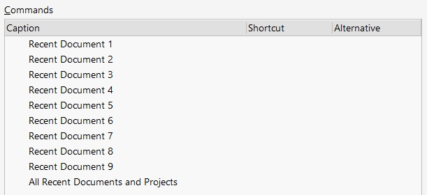
Recent Project Groups: Quick opening of recent project groups.
Let me explain the Recent Project Groups commands in Altium Designer 2025:
Recent Project Groups Commands Overview
These commands provide quick opening of recent project groups or design workspaces, enabling rapid access to collections of related projects and their associated workspace configurations.
Individual Recent Workspace Commands:
Individual Recent Workspaces:
Recent Design Workspace 1 - Opens the most recently used design workspace/project group
Recent Design Workspace 2 - Opens the second most recently used workspace
Recent Design Workspace 3 - Opens the third most recently used workspace
Recent Design Workspace 4 - Opens the fourth most recently used workspace
Recent Design Workspace 5 - Opens the fifth most recently used workspace
Recent Design Workspace 6 - Opens the sixth most recently used workspace
Recent Design Workspace 7 - Opens the seventh most recently used workspace
Recent Design Workspace 8 - Opens the eighth most recently used workspace
Recent Design Workspace 9 - Opens the ninth most recently used workspace
Comprehensive Access:
All Recent Documents and Projects - Shows complete list of all recent documents, projects, and workspaces
What Design Workspaces Include:
Project Collections:
Multiple related projects grouped together
System-level designs with multiple PCBs
Product families with shared components and libraries
Design variants and configuration groups
Workspace Settings:
Panel configurations and layout preferences
Custom toolbars and menu arrangements
Display settings and color schemes
Library paths and component databases
Team Configurations:
Shared workspace settings for team consistency
Collaborative project environments
Standardized workflow configurations
Access permissions and user roles
Key Benefits:
System-Level Design: Manage complex products with multiple interconnected PCBs
Team Collaboration: Maintain consistent workspace settings across team members
Project Organization: Group related projects for efficient management
Workflow Efficiency: Instantly restore complete working environments
Typical Applications:
Multi-Board Systems:
Motherboard + daughtercard combinations
Modular product architectures
System-on-modules with carrier boards
Product Families:
Related products sharing common elements
Design variants with different feature sets
Cost-optimized and performance-optimized versions
Team Projects:
Large projects split among multiple engineers
Collaborative design environments
Standardized team workflows and settings
Usage Workflow:
Recent Design Workspace 1 typically opens your most recent working environment
Use numbered commands to quickly switch between different project groups
All Recent Documents and Projects provides broader access to complete history
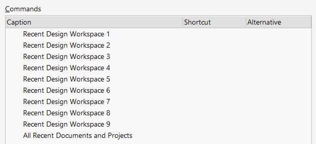
Recent Projects: Quick opening of recent projects.
Recent Projects Commands Overview
These commands provide quick opening of recent projects, allowing rapid access to complete project files you've been working on without navigating through file directories or project browsers.
Individual Recent Project Commands:
Individual Recent Projects:
Recent Project 1 - Opens the most recently accessed project
Recent Project 2 - Opens the second most recently accessed project
Recent Project 3 - Opens the third most recently accessed project
Recent Project 4 - Opens the fourth most recently accessed project
Recent Project 5 - Opens the fifth most recently accessed project
Recent Project 6 - Opens the sixth most recently accessed project
Recent Project 7 - Opens the seventh most recently accessed project
Recent Project 8 - Opens the eighth most recently accessed project
Recent Project 9 - Opens the ninth most recently accessed project
Comprehensive Access:
All Recent Documents and Projects - Shows complete list of recently accessed documents and projects
Provides expanded view beyond the top 9 recent projects
Includes both projects and individual documents
May display additional information like project paths and last modified dates
Types of Recent Projects:
PCB Projects: Complete PCB design projects (.PrjPCB) with schematics and layouts
FPGA Projects: Embedded system projects with FPGA components
Multi-Board Projects: System-level projects with multiple interconnected boards
Library Projects: Projects focused on component library development
Simulation Projects: Projects with extensive simulation and analysis components
Key Benefits:
Project Switching: Instantly switch between different active projects
Workflow Continuity: Resume work exactly where you left off in each project
Multi-Project Management: Efficiently manage multiple concurrent projects
Time Savings: Bypass complex project navigation and file browsing
Typical Usage Scenarios:
Daily Workflow:
Recent Project 1 typically opens your current working project
Use numbered shortcuts for quick access to other active projects
Switch between related projects for system-level designs
Multi-Project Development:
Work on multiple product variations simultaneously
Switch between prototype and production versions
Manage different customer projects efficiently
Team Collaboration:
Quickly access shared team projects
Resume work on assigned project portions
Switch between individual and collaborative projects
Project Loading Features:
Complete Environment: Opens entire project with all associated files
State Restoration: Restores project-specific settings and configurations
Library Loading: Automatically loads project-specific component libraries
Recent File Context: Maintains recently opened documents within each project
Automatic Management:
List updates automatically as you open/close projects
Most recently used projects appear at the top of the list
Maintains history across Altium Designer sessions
Automatically removes invalid or moved project references
These Recent Projects commands are essential for efficient project management, especially when working on multiple concurrent designs or switching between different phases of product development.
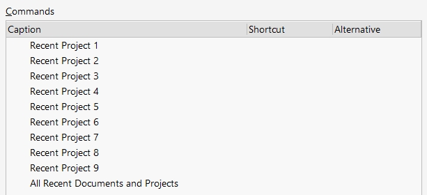
Refactor: Tools for controlled renaming of networks, components, or parameters throughout the project.
Refactor Commands Overview
These tools provide controlled restructuring and reorganization of design elements throughout the project, including moving circuit blocks and converting between different sheet types while maintaining electrical connectivity.
Individual Refactor Commands:
Circuit Block Management:
Move Selected Subcircuit to Different Sheet - Relocates a selected group of components and their connections to a different schematic sheet
Maintains all electrical connections during the move
Preserves component properties and parameters
Updates cross-references and hierarchical connections automatically
Useful for reorganizing large designs or balancing sheet complexity
Sheet Type Conversion:
Convert Schematic Sheet To Device Sheet - Transforms a regular schematic sheet into a device sheet
Changes sheet characteristics and compilation behavior
Updates hierarchical references and connectivity
Maintains component and wiring information
Used for creating reusable device-level circuit blocks
Convert Device Sheet To Schematic Sheet - Converts a device sheet back to a regular schematic sheet
Reverses device sheet characteristics
Updates project hierarchy and references
Preserves all circuit information during conversion
Useful when design requirements change
Key Refactoring Benefits:
Design Organization:
Restructure complex projects for better maintainability
Balance component distribution across multiple sheets
Improve hierarchical design organization
Optimize sheet-level complexity
Hierarchy Management:
Convert between different sheet types as design evolves
Reorganize multi-level hierarchical designs
Adapt sheet structure to match system architecture
Maintain design integrity during restructuring
Project Evolution:
Accommodate changing design requirements
Restructure designs for different team members
Optimize for manufacturing or testing requirements
Adapt legacy designs to new standards
Typical Usage:
Design Restructuring:
Select subcircuit (group of related components)
Use Move Selected Subcircuit to relocate to appropriate sheet
Convert sheet types as needed for proper hierarchy
Verify all connections remain intact
Project Reorganization:
Move power supply circuits to dedicated sheet
Relocate I/O sections for better organization
Balance component density across sheets
Create specialized device sheets for reusable blocks
These refactor commands enable professional design management while maintaining electrical integrity throughout major design restructuring operations.
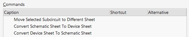
Reports: Generation of various reports (Bill of Materials (BOM), component lists, connection lists in report format).
Reports Commands Overview
These commands generate various reports including Bill of Materials (BOM), component lists, connection lists, and other documentation in report format for design analysis, manufacturing, and project documentation.
Individual Report Commands:
Numbered Report Types (1-30+):
Report 1 through Report 30 - Different pre-configured report types and formats
Each number represents a specific report template or format
Customizable report configurations for different purposes
May include different output formats (PDF, Excel, CSV, HTML)
Pre-configured for various industry standards and requirements
Utility Commands:
Measure Distance (Ctrl+M) - Measures distances between points on the schematic
Automatic Cross References Settings - Configures automatic cross-reference generation for reports
Common Report Types:
Bill of Materials (BOM):
Component lists with quantities and specifications
Part numbers, manufacturers, and supplier information
Cost analysis and procurement data
Assembly and manufacturing information
Component Reports:
Component usage and distribution analysis
Duplicate component identification
Component parameter summaries
Library usage statistics
Connectivity Reports:
Net lists and connection summaries
Pin assignment reports
Signal routing documentation
Cross-reference tables
Design Analysis Reports:
Electrical Rule Check (ERC) results
Design rule violation summaries
Component placement analysis
Signal integrity assessments
Documentation Reports:
Project documentation packages
Design review checklists
Change order documentation
Manufacturing instructions
Key Applications:
Manufacturing Support:
Generate accurate BOMs for component procurement
Create assembly instructions and documentation
Produce quality control checklists
Generate test and inspection reports
Design Verification:
Document design rule compliance
Track component specifications and ratings
Verify connectivity and signal integrity
Generate design review documentation
Project Management:
Cost analysis and budget tracking
Component availability and lead time analysis
Design progress and milestone reporting
Change tracking and version documentation
Typical Workflow:
Complete schematic design and compilation
Select appropriate report number based on required output
Configure report parameters and formatting
Generate report for specific purpose (manufacturing, documentation, analysis)
Export in required format (PDF, Excel, etc.)
Output Formats:
PDF - Professional documentation and printing
Excel/CSV - Data analysis and procurement systems
HTML - Web-based documentation and sharing
Text - Simple listings and data exchange
These report commands are essential for transitioning from design completion to manufacturing, providing all necessary documentation for procurement, assembly, testing, and project management.
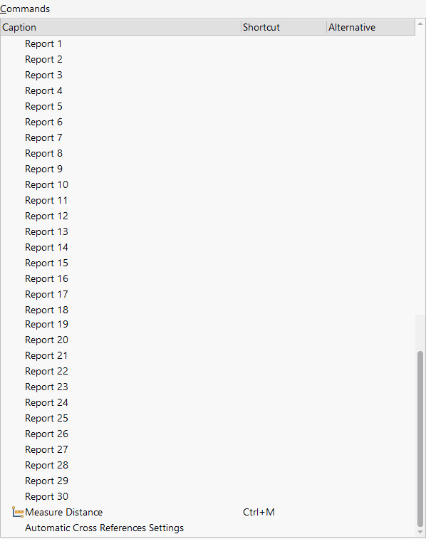
SCH Interactive Shortcuts: Commands that have standard keyboard shortcuts specific to the schematic editor.
Let me explain the SCH Interactive Shortcuts in Altium Designer 2025:
SCH Interactive Shortcuts Overview
These are keyboard shortcuts specific to the schematic editor for rapid interactive operations during schematic design and editing.
Individual Interactive Commands:
Object Manipulation:
Rotate counterclockwise (Space) - Rotates selected objects 90° counterclockwise
Rotate Clockwise (Shift+Space) - Rotates selected objects 90° clockwise
Enlarge (Plus) - Increases size of selected objects
Shrink (Minus) - Decreases size of selected objects
Flip with reference to X-Axis (X) - Mirrors objects horizontally
Flip with reference to Y-Axis (Y) - Mirrors objects vertically
View and Navigation:
Zoom Out (PgDn) - Decreases zoom level
Zoom In (PgUp) - Increases zoom level
Zoom Pan (Home) - Activates pan mode for view navigation
Redraw (End) - Refreshes the display
Editing Operations:
Remove vertex (Backspace, Delete) - Removes vertex points from polygons/lines
Insert vertex (Insert) - Adds vertex points to polygons/lines
Copy from the object under Cursor (Insert) - Copies properties from object under cursor
Cursor Movement:
Move cursor Left (Left) - Moves cursor left
Move cursor Right (Right) - Moves cursor right
Move cursor Up (Up) - Moves cursor up
Move cursor Down (Down) - Moves cursor down
Move cursor Left Fast (Shift+Left) - Moves cursor left in large increments
Move cursor Right Fast (Shift+Right) - Moves cursor right in large increments
Move cursor Up Fast (Shift+Up) - Moves cursor up in large increments
Move cursor Down Fast (Shift+Down) - Moves cursor down in large increments
Wire and Connection Tools:
Toggle wire start/end mode (Space) - Changes wire placement behavior
Cycle wire placement mode (Shift+Space) - Cycles through wire routing modes
Toggle wire start/end mode (Ctrl+Space) - Alternative wire mode toggle
Place bus under intelligent wirer (B) - Places bus with intelligent routing
Place wire under intelligent wirer (W) - Places wire with smart routing
Auto wire type under intelligent wirer (A) - Automatically selects wire type
Net Label Management:
Toggle net label placement position (T) - Changes net label position
Toggle net label name (N) - Toggles net label name display
Turn net label on/off (O) - Shows/hides net labels
Increment port number under intelligent wirer (.) - Increases port numbers
Decrement port number under intelligent wirer (,) - Decreases port numbers
Task and Process Control:
Help (F1) - Opens context-sensitive help
Change through dialog box (Tab) - Opens properties dialog
Abort task (Escape) - Cancels current operation
Pause task (Tab) - Pauses current task
Resume task - Resumes paused task
Complete task (Return) - Completes current operation
Complete task (Ctrl+Return) - Alternative task completion
Sheet Entry Operations:
Reverse Sheet Entry Order (V) - Reverses order of sheet entries
Swap Sheet Entry Side (S) - Moves sheet entries to opposite side
Toggle All Sheet Entry IO Type In Sheet Symbol (T) - Changes I/O types
Toggle Sheet Entry IO (T) - Toggles individual sheet entry I/O direction
Advanced Navigation:
Display popup menu (Shift+F1) - Shows context menu
Subcircuit placement (Shift+S) - Places subcircuit blocks
Next Subcircuit (Shift+N) - Navigates to next subcircuit
Previous Subcircuit (Shift+P) - Navigates to previous subcircuit
Component placement (Shift+C) - Activates component placement mode
Key Benefits:
Speed: Rapid operations without reaching for mouse
Workflow: Smooth interactive editing experience
Precision: Exact object manipulation and positioning
Efficiency: Reduced time for common operations
These interactive shortcuts are essential for productive schematic editing, allowing experienced users to work rapidly while maintaining precision and control.
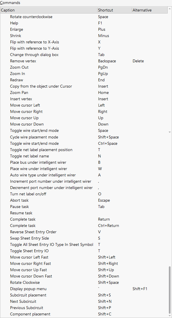
Schematic Active Bar: Commands typically found on the "Active Bar" (context-sensitive toolbar).
Let me explain the Schematic Active Bar commands in Altium Designer 2025:
Schematic Active Bar Commands Overview
These commands are typically found on the "Active Bar" (context-sensitive toolbar) that dynamically changes based on your current schematic editing activity and selected objects.
Individual Active Bar Commands:
Selection and Filtering:
Selection Filter - Controls which types of objects can be selected
Filters selection to specific object types (components, wires, text, etc.)
Helps isolate specific elements during complex editing operations
Prevents accidental selection of unintended objects
Context-sensitive based on current editing task
Component Operations:
Part... - Places components from libraries onto the schematic
Opens component selection dialog
Primary tool for adding components to schematic
Context-sensitive to show recently used or relevant components
Variant Management:
Toggle Fitted/Not Fitted - Toggles component fitting status for design variants
Marks components as fitted or not fitted in current variant
Essential for creating different product configurations
Allows same schematic to represent multiple product versions
Components marked "Not Fitted" are excluded from that variant's BOM
Choose Alternate Part... - Selects alternate components for design variants
Allows different components in different variants
Enables cost optimization or feature differentiation
Maintains same schematic with different component options
Critical for creating product families from single design
Variants - Manages project variants and configurations
Accesses variant management tools
Creates and configures different product versions
Sets up variant-specific parameters and components
Manages fitted/not fitted states across variants
Key Active Bar Characteristics:
Context-Sensitive: Commands change based on selected objects and current tool
Dynamic Content: Available commands adapt to current editing context
Workflow Integration: Provides most relevant tools for current task
Efficiency: Quick access to frequently needed commands
Typical Usage Scenarios:
Component Placement:
Part... appears when placing components
Selection Filter helps select only components during editing
Variant Design:
Toggle Fitted/Not Fitted for components that vary between product versions
Choose Alternate Part for different component options (standard vs. premium parts)
Variants for managing overall variant configurations
Design Organization:
Selection Filter for isolating specific object types during cleanup
Context changes as you switch between different editing tasks
The Active Bar is designed to provide the most relevant tools based on your current schematic editing context, making common operations more accessible and efficient.
Schematic Menu: Commands that populate the main menus of the schematic editor (File, Edit, View, etc.).
Let me explain the Schematic Menu commands in Altium Designer 2025:
Schematic Menu Commands Overview
These commands populate the main menus of the schematic editor (File, Edit, View, etc.) and provide access to general application functions, preferences, and utility features.
Individual Schematic Menu Commands:
Commercial and Support:
Buy Now - Opens purchasing options for Altium Designer licenses and extensions
Access to license upgrades and additional features
Links to Altium's e-commerce platform
Options for subscription renewals and add-ons
Documentation and Annotation:
Place a Comment - Places comment objects on the schematic for documentation
Adds design notes and explanations
Creates review comments and annotations
Documents design decisions and rationale
Essential for team collaboration and design reviews
Sharing and Collaboration:
Share - Provides options for sharing design files and projects
Share via Altium 365 cloud platform
Generate shareable links for design review
Export designs for external collaboration
Team sharing and permission management
Application Access:
Open Home page - Opens Altium Designer's home/start page
Access to recent projects and documents
Quick start templates and tutorials
News and updates from Altium
Central navigation hub
Configuration:
Preferences... - Opens application preferences and settings
Configure schematic editor behavior
Set default colors, fonts, and display options
Customize keyboard shortcuts and interface
Manage library paths and component databases
Essential for personalizing the work environment
Connection Status:
Not Connected - Shows connectivity status (likely to Altium 365 or licensing server)
Indicates current connection state
May provide options to connect/reconnect
Shows licensing and cloud service status
Additional Icons:
Two additional menu items appear to be present but without visible text labels
Likely represent additional utility functions
Could be user profile, help, or system status indicators
Key Menu Categories:
System Functions: Application-level operations and settings
User Support: Help, purchasing, and account management
Collaboration: Sharing and team-based features
Documentation: Annotation and comment tools
Configuration: Preferences and customization options
Typical Usage:
Initial Setup: Use Preferences... to configure Altium Designer for your workflow
Design Documentation: Use Place a Comment for design notes and reviews
Team Collaboration: Use Share for project collaboration and review
Support and Licensing: Use Buy Now and connection status for account management
These menu commands provide the foundational interface elements that support the overall Altium Designer experience beyond the core schematic editing functions.
Schematic Shortcuts: General keyboard shortcuts related to schematics.
Schematic Shortcuts Overview
These are general keyboard shortcuts for common schematic operations, providing rapid access to frequently used commands and tools.
Individual Shortcut Commands:
Basic Editing Operations:
Redo (Ctrl+Y, Ctrl+Backspace) - Reverses last undo operation
Copy (Ctrl+C, Ctrl+Insert) - Copies selected objects to clipboard
Paste (Ctrl+V, Shift+Insert) - Pastes clipboard contents
Cut (Ctrl+X, Shift+Delete) - Cuts selected objects to clipboard
Clear (Delete, Ctrl+Delete) - Deletes selected objects
Duplicate (Ctrl+R) - Creates duplicate of selected objects
View and Navigation:
Zoom In (PgUp) - Increases zoom level
Zoom Out (PgDn) - Decreases zoom level
Fit All Objects (Ctrl+PgDn) - Fits entire schematic in view
Refresh (End) - Redraws the display
Origin (Ctrl+Home) - Centers view on schematic origin
Pan (Home) - Activates pan mode for view navigation
Cursor Movement:
Move Cursor Left/Right/Up/Down Small Step (Arrow keys) - Fine cursor movement
Move Cursor Left/Right/Up/Down Large Step (Shift+Arrow keys) - Coarse cursor movement
Selection Movement:
Move Selection Left/Right/Up/Down Small Step (Ctrl+Arrow keys) - Fine selection movement
Move Selection Left/Right/Up/Down Large Step (Shift+Ctrl+Arrow keys) - Coarse selection movement
Zoom Levels:
100% - Sets zoom to 100% scale
200% - Sets zoom to 200% scale
400% - Sets zoom to 400% scale
50% - Sets zoom to 50% scale
Alignment Tools:
Align Bottom (Shift+Ctrl+B, Ctrl+B) - Aligns objects to bottom edge
Align Left (Shift+Ctrl+L) - Aligns objects to left edge
Align Right (Shift+Ctrl+R) - Aligns objects to right edge
Align Top (Shift+Ctrl+T, Ctrl+T) - Aligns objects to top edge
Align Horizontal Centers - Centers objects horizontally
Distribute Horizontally (Shift+Ctrl+H) - Evenly spaces objects horizontally
Distribute Vertically (Shift+Ctrl+V) - Evenly spaces objects vertically
Align To Grid (Shift+Ctrl+D) - Snaps objects to grid
Text Operations:
Find Text... (Ctrl+F) - Searches for text in schematic
Replace Text... (Ctrl+H, Ctrl+G) - Find and replace text
Find Next (F3) - Continues text search
Object Manipulation:
Move Single Object (Shift+Ctrl+Left_Click) - Moves individual objects
Toggle Single Object Selection (Shift+Left_Click) - Adds/removes from selection
Drag Single Object (Ctrl+Left_Click, Ctrl+Left_Hold_Down) - Drags individual objects
Focus Single Object (Left_Click) - Focuses on single object
Focus and Hold Single Object (Left_Hold_Down) - Maintains focus on object
Interface and Panels:
Main Toolbar - Shows/hides main toolbar
Properties... (Left_Dbl_Click) - Opens properties dialog
Edit In Place (F2) - Enables in-place text editing
Next Tab (Ctrl+TAB) - Switches to next document tab
Previous Tab (Shift+Ctrl+TAB) - Switches to previous document tab
Object Inspector (F11) - Opens object inspector panel
Filter Editor (F12) - Opens filter editor
Object List (Shift+F12) - Shows object list panel
Advanced Tools:
Clear Filter (Shift+C) - Removes active object filters
Clear Underlines (Shift+Ctrl+C) - Removes text underlines
Selection Memory Dialog (Ctrl+Q) - Opens selection memory
Toggle Floating Panels Visibility (F4) - Shows/hides floating panels
Full Screen (Alt+F5) - Toggles full screen mode
Next Channel (Plus) - Navigates to next channel
Previous Channel (Minus) - Navigates to previous channel
Cross Select Mode Reposition Selected Component (Ctrl+Y) - Repositions components
Key Benefits:
Speed: Rapid operations without mouse interaction
Efficiency: Streamlined workflow for common tasks
Precision: Exact cursor and object movement
Professional Workflow: Supports advanced design practices
These shortcuts are essential for efficient schematic design, allowing experienced users to work rapidly while maintaining precision and control over their designs.
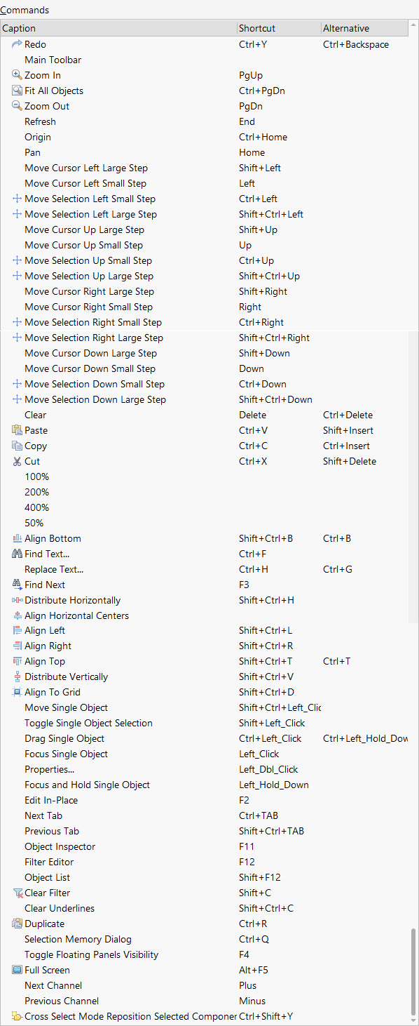
Schematic Standard: Commands typically found on the standard toolbar of the schematic editor.
Let me explain the Schematic Standard commands in Altium Designer 2025:
Schematic Standard Commands Overview
These commands are typically found on the standard toolbar of the schematic editor, providing quick access to the most commonly used functions during schematic design.
Individual Standard Commands:
File Operations:
New (Ctrl+N) - Creates new schematic document
Open... (Ctrl+O) - Opens existing schematic files
Save (Ctrl+S) - Saves current schematic document
Save to Server... (Ctrl+Alt+S) - Saves to version control server
Design Verification:
Component Rule Check - Validates component usage and compliance
Discard Local Changes - Reverts modifications to server version
Output and Documentation:
Print... - Prints schematic documentation
Print Preview... - Shows print preview before printing
PCB Release View - Shows PCB-ready view of the design
View Control:
Workspace (Ctrl+`) - Manages workspace configuration
Fit All Objects (Ctrl+PgDn) - Fits entire schematic in view
Area - Zooms to selected area
Selected Objects - Fits selected objects in view
Color-Coded Selection/Highlighting:
Blue - Assigns blue color coding to objects
Light Green - Assigns light green color coding
Light Blue - Assigns light blue color coding
Red - Assigns red color coding
Fuchsia - Assigns fuchsia/magenta color coding
Yellow - Assigns yellow color coding
Dark Green - Assigns dark green color coding
Basic Editing:
Cut (Ctrl+X, Shift+Delete) - Cuts selected objects
Copy (Ctrl+C, Ctrl+Insert) - Copies selected objects
Paste (Ctrl+V, Shift+Insert) - Pastes clipboard contents
Duplicate (Ctrl+R) - Duplicates selected objects
Selection Management:
Inside Area - Selects objects within defined area
Move Selection - Moves selected objects
All On Current Document - Selects all objects on current sheet
Clear Filter (Shift+C) - Removes active selection filters
History and Navigation:
Undo (Ctrl+Z, Alt+Backspace) - Undoes last operation
Redo (Ctrl+Y, Ctrl+Backspace) - Redoes last undone operation
Up/Down Hierarchy - Navigates hierarchical design levels
Cross Probe - Cross-probes between schematic and other views
Browse Library... - Opens component library browser
Annotation:
Comment... (Ctrl+Alt+C) - Places design comments and notes
Key Characteristics:
Essential Tools: Most frequently used commands during schematic design
Quick Access: One-click access to common operations
Workflow Support: Commands support typical design workflow progression
Visual Feedback: Color coding helps organize and identify objects
Typical Usage:
Design Entry: Use New, Browse Library, and component placement
Editing: Use Cut/Copy/Paste, Duplicate, Undo/Redo
Organization: Use color coding and selection tools for object management
Verification: Use Component Rule Check before proceeding to PCB
Documentation: Use Print and Comment for design documentation
These standard toolbar commands provide the foundation for efficient schematic design by making the most essential tools immediately accessible.
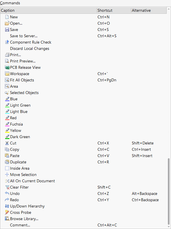
Script: (May be a duplicate or relate to specific script execution, as opposed to managing them) Possibly related to running specific, predefined scripts.
Let me explain the Script commands in Altium Designer 2025:
Script Commands Overview
These commands are related to running specific, predefined scripts or creating new script documents in various scripting languages supported by Altium Designer for automation and customization.
Individual Script Commands:
Project-Level Scripts:
Script Project - Creates or manages scripting projects
Container for multiple related script files
Organizes scripts for complex automation tasks
Manages script dependencies and execution order
General Script Units:
Script Unit - Creates basic script unit files
Generic script file for automation tasks
Foundation for custom Altium Designer automation
Used for repetitive design operations
Script Form - Creates script forms with user interfaces
GUI-based scripts with dialog boxes and controls
User-friendly interfaces for script parameters
Interactive automation tools
Visual Basic Scripts:
VB Script Unit - Creates Visual Basic script files
VBScript-based automation for Altium Designer
Windows-compatible scripting language
Good for users familiar with VB/VBA
VB Script Form - Creates Visual Basic script forms with GUI
VBScript with user interface elements
Dialog-based parameter input
Form-based automation tools
JavaScript Support:
Java Script Unit - Creates JavaScript script files
Modern JavaScript for Altium automation
Cross-platform scripting support
Popular language for many developers
Java Script Form - Creates JavaScript forms with user interface
JavaScript with GUI components
Web-like interface elements
Modern scripting with visual feedback
Specialized Scripts:
TCL Script Unit - Creates TCL (Tool Command Language) script files
TCL scripting for advanced automation
Powerful text processing and system integration
Popular in EDA tool automation
Enable Basic Script Unit - Enables or creates basic script functionality
Simple scripting capability activation
Entry-level automation features
Basic script execution environment
Key Applications:
Design Automation:
Automate repetitive schematic operations
Batch processing of multiple designs
Custom component placement and routing
Automated report generation
Custom Tools:
Create specialized design utilities
Build company-specific design rules
Develop custom analysis tools
Create design verification scripts
Integration:
Interface with external databases
Connect to company design systems
Automate design handoff processes
Generate custom documentation
Typical Script Uses:
Component Management: Automated component placement and property updates
Documentation: Custom report generation and formatting
Design Rules: Company-specific design rule checking
File Processing: Batch operations on multiple design files
Integration: Connect Altium to other business systems
These script commands enable powerful customization and automation capabilities, allowing users to extend Altium Designer's functionality for specific workflows and requirements.
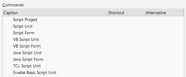
Select: Commands for selecting objects (Select All, Select Inside Area, Select Objects Touching Line, etc.).
Select Commands Overview
These commands provide various methods for selecting objects in the schematic, including area-based selection, connection-based selection, and selection manipulation tools.
Individual Select Commands:
Area-Based Selection:
Lasso Select - Selects objects by drawing a freeform lasso around them
Draw any shape around objects to select them
Flexible selection for irregularly positioned objects
Useful for selecting complex groups of components
Inside Area - Selects all objects completely inside a defined rectangular area
Objects must be entirely within the selection rectangle
Precise selection for clean rectangular regions
Excludes objects that cross the boundary
Outside Area - Selects all objects that are completely outside a defined area
Inverse of Inside Area selection
Selects everything except objects in defined region
Useful for selecting background elements
Boundary-Based Selection:
Touching Rectangle - Selects objects that touch or intersect with a rectangular selection area
Includes objects that cross the selection boundary
More inclusive than Inside Area selection
Standard "crossing window" selection behavior
Touching Line - Selects objects that touch or cross a drawn line
Draw a line to select intersecting objects
Useful for selecting objects along a path
Good for selecting wires, components, or text along a route
Global Selection:
All (Ctrl+A) - Selects all objects on the current schematic sheet
Universal selection of every object
Starting point for global operations
Most commonly used selection command
Connection-Based Selection:
Connection - Selects electrically connected objects
Follows electrical connections (nets) to select related objects
Selects entire networks including components, wires, and labels
Essential for tracing signal paths and connectivity
Selection Management:
Toggle Selection - Inverts the current selection state
Selected objects become deselected
Deselected objects become selected
Useful for selecting everything except current selection
Key Benefits:
Flexibility: Multiple selection methods for different scenarios
Precision: Choose appropriate selection method for specific tasks
Efficiency: Rapid selection of complex object groups
Workflow Support: Selection methods match common editing patterns
Typical Usage:
Component Groups: Use Lasso Select for irregularly arranged components
Rectangular Areas: Use Inside Area for clean rectangular selections
Network Tracing: Use Connection to select entire electrical networks
Global Operations: Use All (Ctrl+A) for document-wide operations
Inverse Selection: Use Toggle Selection to select everything except current selection
Common Workflows:
Use Connection to select and highlight entire nets
Use Inside Area to select components in specific circuit blocks
Use All followed by Toggle Selection to select everything except specific objects
Use Touching Line to select objects along routing paths
These selection commands are fundamental to efficient schematic editing, providing the precision and flexibility needed for professional electronic design work.
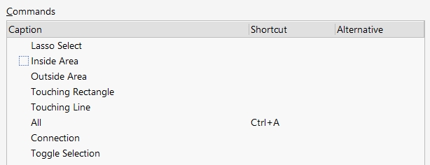
Set Location Marks: Commands for defining location marks.
Set Location Marks Commands Overview
These commands define and save location marks (bookmarks) at specific positions in the schematic, creating reference points that can be quickly recalled later for navigation.
Individual Set Location Mark Commands:
Numbered Location Mark Slots (1-10):
Set Location Mark 1 - Saves current view position as bookmark #1
Set Location Mark 2 - Saves current view position as bookmark #2
Set Location Mark 3 - Saves current view position as bookmark #3
Set Location Mark 4 - Saves current view position as bookmark #4
Set Location Mark 5 - Saves current view position as bookmark #5
Set Location Mark 6 - Saves current view position as bookmark #6
Set Location Mark 7 - Saves current view position as bookmark #7
Set Location Mark 8 - Saves current view position as bookmark #8
Set Location Mark 9 - Saves current view position as bookmark #9
Set Location Mark 10 - Saves current view position as bookmark #10
How Set Location Marks Work:
Setting Location Marks:
Navigate to desired position in schematic
Set appropriate zoom level and view area
Execute Set Location Mark command for desired slot number
Current view state is saved to that numbered bookmark
Saved Information:
Position: Exact X,Y coordinates of view center
Zoom Level: Current magnification level
Display Settings: Layer visibility and display options (depending on implementation)
Key Benefits:
Navigation Efficiency: Create bookmarks for important circuit areas
Design Organization: Mark different functional blocks for quick access
Review Process: Set bookmarks at key review points
Multi-Area Work: Efficiently work across different sections of large designs
Typical Usage Workflow:
Setting Up Navigation Points:
Navigate to power supply section → Set Location Mark 1
Navigate to microcontroller area → Set Location Mark 2
Navigate to I/O connectors → Set Location Mark 3
Navigate to analog front-end → Set Location Mark 4
Continue for other important areas
Strategic Bookmark Placement:
Mark 1: Main processor/controller section
Mark 2: Power supply and regulation
Mark 3: Input/output interfaces
Mark 4: Communication circuits
Mark 5: Analog signal processing
Mark 6: Clock generation and timing
Mark 7: Test points and debugging
Mark 8: Critical signal paths
Mark 9: Problem areas under review
Mark 10: Reference designs or notes
Relationship to Recall Commands:
Set Location Marks: Define and store bookmarks (these commands)
Recall Location Marks: Jump to stored bookmarks (Alt+1 through Alt+10)
This bookmark system significantly improves productivity when working with large, complex schematics by eliminating repetitive navigation and allowing instant access to important design areas.
Set Net Colors: Tools for assigning custom colors to networks for better visualization.
Set Net Colors Commands Overview
These tools assign custom colors to networks (electrical connections) for better visualization, signal identification, and schematic organization.
Individual Set Net Colors Commands:
Predefined Color Schemes:
Set Net Colors 1 - Applies predefined color scheme #1 to selected networks
Set Net Colors 2 - Applies predefined color scheme #2 to selected networks
Set Net Colors 3 - Applies predefined color scheme #3 to selected networks
Set Net Colors 4 - Applies predefined color scheme #4 to selected networks
Set Net Colors 5 - Applies predefined color scheme #5 to selected networks
Set Net Colors 6 - Applies predefined color scheme #6 to selected networks
Set Net Colors 7 - Applies predefined color scheme #7 to selected networks
Custom Configuration:
Custom... - Opens custom color selection dialog for networks
Choose specific colors for individual nets or net groups
Create custom color schemes for specific design requirements
Configure colors based on signal types or functionality
Color Management:
Clear Net Color - Removes color assignment from selected networks
Returns nets to default schematic colors
Allows selective color removal
Useful for cleaning up color assignmentsм
Clear All Net Colors - Removes all network color assignments from the schematic
Resets entire schematic to default colors
Clears all custom color schemes at once
Useful for starting fresh with color assignmentsм
Key Applications:
Signal Type Identification:
Power Nets: Red colors for power supply connections
Ground Nets: Black or dark colors for ground connections
Clock Signals: Blue colors for timing-critical signals
Data Buses: Green colors for data transmission lines
Control Signals: Purple or orange for control and enable lines
Functional Grouping:
Analog Signals: One color family for analog circuits
Digital Signals: Different color family for digital logic
High-Speed Signals: Distinctive colors for critical timing paths
Low-Speed Signals: Subdued colors for non-critical connections
Design Review and Debugging:
Problem Nets: Bright colors to highlight problematic connections
Critical Paths: High-contrast colors for important signal routing
Test Points: Special colors for debugging and measurement points
Optional Circuits: Faded colors for variant or optional connections
Typical Usage Workflow:
Setting Up Color Coding:
Select networks by clicking on wires or using net selection tools
Choose appropriate Set Net Colors command based on signal type
Use Custom... for specific color requirements
Repeat for different signal groups
Common Color Assignments:
Set Net Colors 1: Power supply nets (VCC, VDD) - Red
Set Net Colors 2: Ground nets (GND, VSS) - Black/Dark
Set Net Colors 3: Clock and timing signals - Blue
Set Net Colors 4: Data buses and communication - Green
Set Net Colors 5: Control and enable signals - Orange
Set Net Colors 6: Analog signals - Purple
Set Net Colors 7: Special or test signals - Yellow
Benefits:
Visual Organization: Instantly identify signal types and functions
Design Review: Easier schematic review and verification
Debugging: Quick identification of signal paths during troubleshooting
Documentation: Professional appearance with logical color coding
Team Collaboration: Consistent color standards across team members
These net color commands significantly improve schematic readability and help maintain organized, professional designs that are easier to understand, review, and debug.
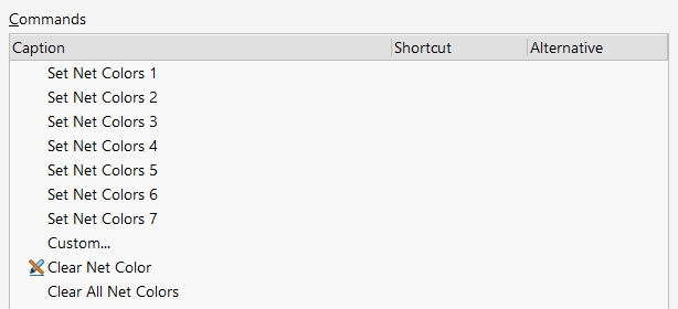
Sheet Symbols: Commands for placing and managing sheet symbols for hierarchical design.
Let me explain the Sheet Symbols commands in Altium Designer 2025:
Sheet Symbols Commands Overview
These commands handle placing and managing sheet symbols for hierarchical design, enabling modular schematic organization where complex designs are broken into manageable, interconnected sheets.
Individual Sheet Symbol Commands:
Basic Hierarchical Elements:
Sheet Symbol - Places hierarchical sheet symbols on the parent schematic
Represents entire child schematic sheets as single symbols
Creates hierarchical design structure for complex projects
Essential for modular design methodology
Allows system-level view with detailed sub-circuits
Sheet Entry - Creates connection points (pins) on sheet symbols
Defines electrical interface between parent and child sheets
Creates input/output ports on sheet symbol boundaries
Establishes signal flow between hierarchical levels
Critical for maintaining electrical connectivity across hierarchy
Specialized Sheet Types:
Device Sheet Symbol - Places device-specific sheet symbols
Represents hardware devices or subsystems as hierarchical blocks
Used for complex components that require detailed internal schematics
Suitable for FPGA, microprocessor, or complex IC representations
Maintains device-level organization within system hierarchy
Reusable Design Elements:
Reuse Block... - Places reusable circuit blocks
Pre-designed circuit sections that can be used multiple times
Standardized circuits for common functions (power supplies, interfaces)
Promotes design consistency and reduces development time
Enables library of proven circuit designs
Hierarchical Design Benefits:
Design Organization:
Break complex designs into manageable sheets
Create logical functional groupings
Maintain system-level overview while enabling detailed design
Support team-based design where different engineers work on different sheets
Scalability:
Handle large designs with hundreds of components
Organize multi-board systems efficiently
Support product families with shared sub-circuits
Enable incremental design development
Reusability:
Create standard circuit blocks for repeated use
Maintain consistent implementations across projects
Reduce design time through proven sub-circuits
Enable design libraries for company standards
Typical Hierarchical Workflow:
System Design:
Create top-level schematic with Sheet Symbol blocks
Add Sheet Entry points for each sheet symbol interface
Create corresponding child sheets for each sheet symbol
Design detailed circuits within each child sheet
Common Hierarchy Examples:
Power Management Sheet: Voltage regulators and power distribution
Processor Sheet: CPU, memory, and core support circuits
I/O Interface Sheet: Connectors and interface circuits
Communication Sheet: Ethernet, USB, or wireless circuits
Analog Frontend Sheet: Sensors and analog signal processing
Device Integration:
Use Device Sheet Symbol for complex ICs requiring detailed pin assignments
Create Reuse Block elements for standard interface circuits
Maintain consistent interfaces across all hierarchical levels
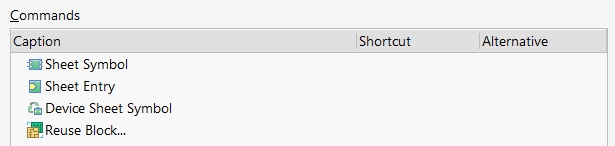
Sheet Templates: Applying or managing templates for schematic sheets (e.g., frames, title blocks).
Sheet Templates Commands Overview
These commands apply or manage templates for schematic sheets, including frames, title blocks, borders, and other standardized formatting elements that provide professional documentation structure.
Individual Sheet Template Commands:
Template Sources:
Local - Applies templates stored locally on your computer
Uses templates from local file system
Personal or project-specific template files
Custom templates created for specific needs
Independent of server connectivity
Server - Applies templates stored on company server or Altium 365
Uses centralized company-standard templates
Ensures consistency across team designs
Automatically updated company branding and standards
Requires server connection for access
Template Management:
Set Template from server... - Configures which server template to apply
Browse and select from available server templates
Choose appropriate template for project type
Configure template parameters and settings
Establish connection to template source
Update Current Template... - Updates the currently applied template
Refreshes template with latest version from source
Maintains template consistency across project
Updates company branding or standard changes
Preserves existing schematic content while updating format
Remove Current Template... - Removes template from current schematic sheet
Returns sheet to basic format without template
Removes title blocks, borders, and standard elements
Useful for creating custom or simplified formats
Allows template-free design when needed
What Sheet Templates Include:
Professional Documentation Elements:
Title Blocks: Company logos, project information, revision history
Border Frames: Standard sheet boundaries and reference grids
Drawing Standards: Line weights, text sizes, standard symbols
Revision Tracking: Areas for design change documentation
Company Branding: Logos, contact information, standard formatting
Information Fields:
Project name and description
Designer and checker names
Drawing numbers and sheet numbers
Date and revision information
Approval signatures and dates
Key Applications:
Company Standards: Ensure all designs meet company documentation requirements
Professional Appearance: Create publication-ready schematic documentation
Compliance: Meet industry standards for technical documentation
Consistency: Maintain uniform appearance across all project sheets
Typical Usage Workflow:
Initial Setup:
Use Server or Local to apply appropriate company template
Configure template parameters for specific project
Template automatically adds title blocks, borders, and standard elements
Template Management:
Use Update Current Template when company standards change
Use Set Template from server to change template types
Use Remove Current Template for special formatting requirements
Team Collaboration:
Server templates ensure all team members use same standards
Automatic updates maintain consistency across all designs
Company branding and standards automatically applied
Benefits:
Professional Documentation: Creates publication-ready technical drawings
Time Savings: Eliminates manual creation of title blocks and borders
Consistency: Ensures uniform appearance across all company designs
Compliance: Meets industry and company documentation standards
Branding: Maintains company identity in all technical documentation
These template commands are essential for creating professional, standardized schematic documentation that meets industry and company requirements.
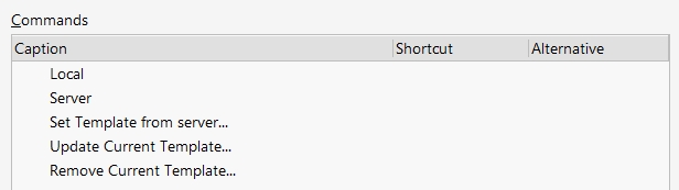
Simulate: General simulation control commands (Run, Stop, Pause).
Let me explain the Simulate commands in Altium Designer 2025:
Simulate Commands Overview
These are general simulation control commands (Run, Stop, Pause) for controlling circuit simulation and analysis within Altium Designer's integrated simulation environment.
Individual Simulate Commands:
Multiple Simulation Profiles:
Run Simulator1 through Run Simulator9 - Executes different simulation configurations
Each numbered simulator represents a different simulation setup or profile
Pre-configured analysis types (DC, AC, Transient, etc.)
Different simulation parameters and conditions
Allows multiple simulation scenarios for the same circuit
Primary Simulation Control:
Run Simulation (F9) - Executes the main simulation analysis
Primary command for starting circuit simulation
Runs currently configured simulation analysis
Most commonly used simulation command
Quick keyboard access with F9
Simulation Management:
Simulation Dashboard - Opens the simulation control and monitoring interface
Central control panel for all simulation operations
Real-time monitoring of simulation progress
Waveform viewing and analysis tools
Parameter adjustment and control interface
Simulation Setup:
Place Simulation Generic Component - Adds generic simulation elements
Places simulation-specific components (voltage sources, loads, etc.)
Components that exist only for simulation purposes
Test and measurement elements for analysis
Stimulus generators and measurement probes
Place Initial Condition - Sets initial circuit conditions for simulation
Defines starting values for capacitor voltages
Sets initial inductor currents
Establishes node voltages at simulation start
Critical for transient analysis accuracy
Netlist Generation:
Generate Netlist - Creates simulation netlist from schematic
Converts schematic to SPICE-compatible netlist
Includes all component models and connections
Required step before simulation execution
Validates circuit for simulation compatibility
Common Simulation Types:
DC Analysis: Operating point and DC sweep analysis
AC Analysis: Frequency response and small-signal analysis
Transient Analysis: Time-domain behavior and switching analysis
Noise Analysis: Circuit noise performance evaluation
Monte Carlo Analysis: Statistical variation analysis
Typical Simulation Workflow:
Setup Phase:
Add simulation sources using Place Simulation Generic Component
Set Place Initial Condition where needed
Configure analysis parameters for each simulator profile
Generate Netlist to prepare for simulation
Execution Phase:
Select appropriate simulator (1-9) based on analysis type
Use Run Simulation (F9) or specific simulator command
Monitor progress through Simulation Dashboard
Analyze results in waveform viewers
Analysis Types by Simulator:
Simulator1: DC operating point analysis
Simulator2: AC frequency response
Simulator3: Transient time-domain
Simulator4: Noise analysis
Simulator5: Monte Carlo statistical
Simulator6-9: Custom or specialized analyses
Key Benefits:
Pre-Verification: Validate circuit behavior before physical prototyping
Optimization: Fine-tune component values and circuit performance
Design Validation: Ensure specifications are met across all conditions
Cost Reduction: Reduce prototype iterations through simulation
These simulation commands enable comprehensive circuit analysis and verification, critical for developing reliable electronic designs before committing to physical implementation.

Simulation Tools: A broader set of tools related to simulation setup and analysis.
Let me explain the Simulation Tools commands in Altium Designer 2025: Simulation Tools Commands Overview This is a broader set of tools related to simulation setup and analysis, providing the essential elements needed to create, stimulate, and measure circuits during simulation. Individual Simulation Tool Commands: Simulation Sources (Stimulus): Voltage Source - Places voltage sources for circuit stimulation DC, AC, pulse, sine wave, and custom waveform generators Essential for powering circuits during simulation Configurable amplitude, frequency, and waveform parameters Primary stimulus for most circuit simulations Current Source - Places current sources for circuit analysis DC and AC current generators Used for current-mode circuit analysis Bias current injection for analog circuits Testing current-driven circuit behaviorSimulation Generic Component - Places generic simulation elements
Specialized simulation-only components
Test loads, switches, and measurement devices
Components that don't exist in real circuits
Simulation-specific modeling elements
Measurement Probes:
Voltage Probe - Measures voltage at specific circuit nodes
Single-ended voltage measurement relative to ground
Essential for monitoring signal levels and DC operating points
Shows voltage waveforms in simulation results
Most commonly used measurement tool
Voltage Diff Probe - Measures differential voltage between two points
Voltage difference measurement between any two nodes
Critical for differential signal analysis
Measures voltage drops across components
Important for op-amp and differential circuit analysis
Current Probe - Measures current flow through circuit branches
Measures current flowing through wires or component leads
Essential for power analysis and current verification
Shows current waveforms during simulation
Critical for component stress analysis
Power Probe - Measures power consumption or dissipation
Calculates instantaneous and average power
Essential for power efficiency analysis
Battery life estimation in portable designs
Thermal analysis and component derating
Initial Conditions:
Initial Condition - Sets starting conditions for simulation
Defines initial capacitor voltages
Sets initial inductor currents
Establishes node voltages at simulation start
Critical for transient analysis convergence
Simulation Setup Workflow:
Step 1: Add Stimulus Sources
Place Voltage Source for power supply connections
Add Voltage Source for input signal generation
Use Current Source for bias currents where needed
Step 2: Place Measurement Probes
Add Voltage Probe at critical circuit nodes
Place Current Probe to monitor current flow
Use Power Probe for efficiency analysis
Add Voltage Diff Probe for differential measurements
Step 3: Configure Initial Conditions
Set Initial Condition for energy storage elements
Define starting voltages for capacitors
Set initial currents for inductors
Step 4: Run Simulation
Generate netlist and execute simulation
View probe results in waveform viewer
Analyze circuit performance
Key Applications:
Circuit Verification: Validate design meets specifications
Performance Analysis: Optimize component values and circuit behavior
Stress Analysis: Ensure components operate within ratings
Power Analysis: Optimize power consumption and efficiency
Signal Integrity: Verify signal quality and timing
These simulation tools provide comprehensive circuit analysis capabilities, enabling thorough design verification before physical prototyping.
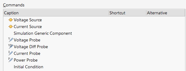
Simulator: Specific commands for interacting with the simulation engine.
Let me explain the Simulator commands in Altium Designer 2025:
Simulator Commands Overview
These are specific commands for interacting with the simulation engine, providing direct control over simulation environment setup, configuration, and testbench management.
Individual Simulator Command:
Testbench Management:
Manage Testbenches... - Opens testbench management interface for simulation control
Creates and configures simulation testbenches
Manages multiple test scenarios for the same circuit
Sets up stimulus patterns and measurement configurations
Organizes different simulation experiments and conditions
What Testbenches Include:
Test Environment Setup:
Stimulus Configuration: Define input signals, power supplies, and test conditions
Measurement Setup: Configure probes, analysis types, and output parameters
Simulation Parameters: Set analysis types, time ranges, and convergence criteria
Test Scenarios: Multiple test cases for different operating conditions
Simulation Control:
Analysis Types: DC, AC, Transient, Noise, Monte Carlo configurations
Sweep Parameters: Variable component values or operating conditions
Corner Analysis: Best case, worst case, and typical condition testing
Statistical Analysis: Process variation and tolerance studies
Key Testbench Applications:
Design Verification:
Functional verification under various operating conditions
Performance characterization across temperature and voltage ranges
Stress testing at component limits
Compliance testing against specifications
Optimization Studies:
Component value optimization for best performance
Trade-off analysis between different design parameters
Yield analysis and design centering
Power consumption optimization
Production Testing:
Test patterns for manufacturing verification
Go/no-go criteria for production units
Automated test sequence generation
Quality control validation
Typical Testbench Workflow:
Setup Phase:
Use Manage Testbenches... to create new testbench
Configure stimulus sources and operating conditions
Set up measurement probes and analysis parameters
Define pass/fail criteria and expected results
Execution Phase:
Run testbench simulations automatically
Collect and analyze results across all test conditions
Generate reports and performance summaries
Validate design meets all requirements
Advanced Testbench Features:
Parametric Sweeps: Automatically vary component values
Corner Analysis: Test across process, voltage, temperature (PVT) corners
Monte Carlo: Statistical analysis with component tolerances
Multi-Configuration: Test different circuit variants simultaneously
Benefits:
Automation: Reduces manual simulation setup for repetitive testing
Consistency: Ensures systematic testing across all design requirements
Documentation: Maintains test procedures and results for design reviews
Efficiency: Streamlines complex simulation workflows
The Manage Testbenches... command provides professional-level simulation management capabilities essential for thorough design verification and optimization in complex electronic designs.
Store: Possibly saving current views or settings.
Store Commands Overview
These commands save current views or settings to numbered memory slots, creating bookmarks that can be quickly recalled later for efficient navigation and workflow management.
Individual Store Commands:
Numbered Storage Slots (1-8):
Store 1 (Ctrl+1, Ctrl+Num1) - Saves current view/setting to memory slot #1
Store 2 (Ctrl+2, Ctrl+Num2) - Saves current view/setting to memory slot #2
Store 3 (Ctrl+3, Ctrl+Num3) - Saves current view/setting to memory slot #3
Store 4 (Ctrl+4, Ctrl+Num4) - Saves current view/setting to memory slot #4
Store 5 (Ctrl+5, Ctrl+Num5) - Saves current view/setting to memory slot #5
Store 6 (Ctrl+6, Ctrl+Num6) - Saves current view/setting to memory slot #6
Store 7 (Ctrl+7, Ctrl+Num7) - Saves current view/setting to memory slot #7
Store 8 (Ctrl+8, Ctrl+Num8) - Saves current view/setting to memory slot #8
What Gets Stored:
View Information:
Current zoom level and magnification
Pan position and view center coordinates
Visible area and focus point
Display settings and layer visibility
State Information:
Current selection states
Active tool and mode settings
Panel configurations and workspace layout
Filter settings and display options
Relationship with Recall Commands:
Store Commands (Ctrl+1-8): Save current state to numbered slots
Recall Commands (Alt+1-8): Restore previously saved states from those slots
This creates a powerful bookmark system for rapid navigation and state management.
Typical Usage Workflow:
Setting Up Memory Slots:
Navigate to power supply section, set appropriate zoom
Press Ctrl+1 to store this view as memory slot 1
Navigate to I/O interface area
Press Ctrl+2 to store this view as memory slot 2
Continue for other important areas
Working with Stored Views:
Press Alt+1 to quickly jump to power supply area
Press Alt+2 to instantly view I/O interfaces
Press Alt+3 for other stored locations
Update stored views by repeating Store commands
Strategic Memory Management:
Common Storage Assignments:
Store 1: Main system overview
Store 2: Power supply and regulation circuits
Store 3: Microcontroller/processor section
Store 4: I/O connectors and interfaces
Store 5: Communication circuits (Ethernet, USB, etc.)
Store 6: Analog front-end and sensors
Store 7: Clock generation and timing
Store 8: Test points and debugging areas
Key Benefits:
Navigation Efficiency: Instantly return to important design areas
Workflow Optimization: Eliminate repetitive zoom and pan operations
Design Review: Quick access to review checkpoints
Multi-Area Work: Efficiently switch between different circuit sections
Integration with Design Process:
Initial Design: Store key areas during component placement
Routing Phase: Store critical signal areas and connection points
Review Process: Store problem areas and verification points
Documentation: Store areas for screenshot and documentationv
These Store commands, combined with their corresponding Recall commands, provide a powerful navigation system that significantly improves productivity when working with large, complex schematic designs.
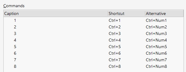
Store Plus: Advanced version of the "Store" command.
Store Plus Commands Overview
These are advanced versions of the standard "Store" commands, providing enhanced state storage capabilities with more comprehensive information capture and sophisticated bookmark management.
Individual Store Plus Commands:
Numbered Enhanced Storage Slots (1-8):
Store Plus 1 (Shift+1, Shift+Num1) - Saves comprehensive state to enhanced memory slot #1
Store Plus 2 (Shift+2, Shift+Num2) - Saves comprehensive state to enhanced memory slot #2
Store Plus 3 (Shift+3, Shift+Num3) - Saves comprehensive state to enhanced memory slot #3
Store Plus 4 (Shift+4, Shift+Num4) - Saves comprehensive state to enhanced memory slot #4
Store Plus 5 (Shift+5, Shift+Num5) - Saves comprehensive state to enhanced memory slot #5
Store Plus 6 (Shift+6, Shift+Num6) - Saves comprehensive state to enhanced memory slot #6
Store Plus 7 (Shift+7, Shift+Num7) - Saves comprehensive state to enhanced memory slot #7
Store Plus 8 (Shift+8, Shift+Num8) - Saves comprehensive state to enhanced memory slot #8
Enhanced Storage Capabilities:
Comprehensive View State:
More detailed zoom and pan information than standard Store
Layer visibility states and display configurations
Panel arrangements and workspace layout
Multi-document view states (across multiple schematic sheets)
Advanced Context Information:
Selection states and active filters
Cross-reference states and navigation history
Object highlighting and color assignments
Search and filter criteria settings
Complex Design States:
Hierarchical design position tracking
Multi-sheet design context and relationships
Project-wide view state management
Advanced analysis and measurement configurations
Key Differences from Standard Store:
More Comprehensive: Captures significantly more design state information
Enhanced Shortcuts: Uses Shift+Number combinations for advanced functionality
Complex State Management: Handles multi-parameter and multi-document states
Professional Workflow: Designed for sophisticated, multi-sheet professional designs
Relationship with Recall Plus:
Store Plus Commands (Shift+1-8): Save enhanced states to memory slots
Recall Plus Commands (Shift+Alt+1-8): Restore comprehensive saved states
This creates an advanced bookmark system for complex professional workflows.
Typical Advanced Usage:
Complex Design Review States:
Set up comprehensive review state (zoom, selections, filters, multiple sheets)
Use Store Plus 1 (Shift+1) to save complete state
Later use Recall Plus 1 (Shift+Alt+1) to restore entire review environment
Multi-Sheet Design Navigation:
Store Plus 1: Complete system overview state across multiple sheets
Store Plus 2: Power distribution analysis state with filters and highlights
Store Plus 3: Signal integrity review state with cross-references
Store Plus 4: Component placement verification state with selection filters
Advanced Analysis States:
Save complex filter combinations with specific analysis views
Store cross-reference states for hierarchical design navigation
Maintain sophisticated selection states across multiple design documents
Preserve advanced measurement and probing configurations
Professional Applications:
Design Reviews: Save complete review states for collaborative sessions
Complex Debugging: Store comprehensive debugging states with multiple views
Team Collaboration: Share complex design states for collaborative analysis
Advanced Workflows: Support sophisticated multi-sheet design methodologies
These Store Plus commands provide power users with enhanced state management capabilities essential for managing complex professional design workflows that require preservation of sophisticated design contexts and multi-parameter states.
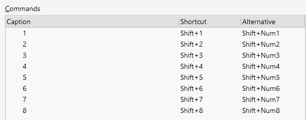
Text Tools: Commands for manipulating text objects (font, size, alignment, find/replace text).
Individual Text Tool Commands:
Basic Text Elements:
Text String - Places basic text labels and annotations on the schematic
Simple text objects for component labels, notes, and general annotation
Configurable font, size, color, and style properties
Used for circuit documentation, reference designators, and explanatory text
Essential for adding descriptive information to schematics
Text Frame - Creates bordered text areas with frames around text content
Text with visible rectangular borders or frames
Used for important notes, warnings, or highlighted information
Provides visual emphasis and organization for critical text
Professional appearance for formal documentation
Note - Places design notes and comments with specialized formatting
Specialized text objects for design documentation
May include automatic numbering or special formatting
Used for design rationale, change notes, and review comments
Often linked to design revision tracking
Key Text Manipulation Features:
Font and Appearance:
Font family selection (Arial, Times, etc.)
Font size adjustment for readability
Bold, italic, and underline text styling
Color assignment for text categorization
Rotation and orientation control
Alignment and Positioning:
Left, center, right text alignment
Vertical alignment options
Precise positioning and spacing
Grid alignment and snapping
Consistent text placement
Content Management:
Find and replace text across entire schematic
Global text property updates
Batch text formatting changes
Text content search and modification
Pattern-based text replacement
Common Text Applications:
Circuit Documentation:
Component value labels and specifications
Signal names and descriptions
Operating conditions and ratings
Design notes and explanations
Schematic Annotation:
Test point identification
Connector pin assignments
Revision notes and change documentation
Reference information and calculations
Professional Documentation:
Title block information
Drawing notes and specifications
Safety warnings and cautions
Compliance and certification notes
Typical Usage Workflow:
Basic Annotation:
Use Text String for general labels and component annotations
Configure appropriate font size for readability
Position text for clear association with components
Important Information:
Use Text Frame for critical notes requiring visual emphasis
Configure border style and text formatting
Position prominently for visibility
Design Documentation:
Use Note for formal design documentation
Include revision information and design rationale
Link to specific design elements or changes
Text Management Benefits:
Professional Appearance: Consistent text styling across all schematics
Documentation Quality: Clear, readable technical documentation
Design Communication: Effective information transfer to team members
Standards Compliance: Meet industry documentation requirements
These Text Tools are essential for creating professional, well-documented schematics that clearly communicate design intent and provide necessary technical information for manufacturing, testing, and maintenance.
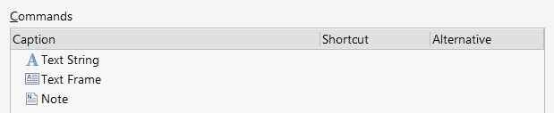
Toolbars: Commands for displaying/hiding specific toolbars.
Let me explain the Toolbars commands in Altium Designer 2025:
Toolbars Commands Overview
These commands control the display and hiding of specific toolbars in the Altium Designer interface, allowing users to customize their workspace by showing only the toolbars they need for their current workflow.
Individual Toolbar Commands:
Numbered Toolbar Toggle Commands (1-16):
Toggle Toolbar 1 through Toggle Toolbar 16 - Show/hide specific toolbars
Each number represents a different functional toolbar in the interface
Toggle functionality allows quick show/hide to optimize screen space
Context-sensitive toolbars that appear based on current editing mode
Customizable toolbar arrangements for different workflow needs
Toolbar Customization:
Customize... - Opens toolbar customization dialog
Configure which toolbars are available
Customize toolbar content and button arrangements
Create custom toolbar layouts for specific workflows
Manage toolbar positioning and docking options
Common Altium Designer Toolbars:
Core Design Toolbars:
Standard Toolbar: File operations, basic editing, and common commands
Schematic Toolbar: Schematic-specific placement and editing tools
Wiring Toolbar: Wire, bus, and connection placement tools
Align Toolbar: Object alignment and distribution tools
Specialized Function Toolbars:
Simulation Toolbar: Simulation setup and control commands
Annotation Toolbar: Component annotation and numbering tools
Drawing Tools Toolbar: Graphic primitives and drawing elements
Text Toolbar: Text placement and formatting tools
View and Navigation Toolbars:
View Toolbar: Zoom, pan, and display control
Grid Toolbar: Grid management and snap settings
Layer Toolbar: Layer visibility and management
Selection Toolbar: Object selection and filtering tools
Key Benefits:
Workspace Optimization: Show only relevant toolbars for current task
Screen Space Management: Maximize schematic viewing area by hiding unused toolbars
Workflow Efficiency: Quick access to frequently used tools
Customization: Tailor interface to personal preferences and work habits
Typical Usage Scenarios:
Schematic Entry Phase:
Show Standard, Schematic, and Wiring toolbars
Hide simulation and analysis toolbars
Focus on component placement and connection tools
Design Review Phase:
Show View, Selection, and Annotation toolbars
Hide placement and drawing toolbars
Emphasize navigation and analysis tools
Documentation Phase:
Show Text, Drawing Tools, and Align toolbars
Focus on annotation and graphic enhancement tools
Hide design-specific placement toolbars
Simulation Phase:
Show Simulation and Analysis toolbars
Keep View toolbar for result examination
Hide placement and routing toolbars
Workspace Management:
Task-Specific Configurations:
Save different toolbar configurations for different design phases
Switch between toolbar setups based on current work
Optimize screen real estate for different monitor sizes
Create team-standard toolbar arrangements
Customization Workflow:
Use Customize... to access toolbar management
Configure which toolbars are available
Use Toggle Toolbar commands for quick show/hide
Arrange toolbars for optimal workflow efficiency
These toolbar commands enable users to create efficient, personalized workspaces that adapt to different phases of the electronic design process, maximizing productivity by providing quick access to relevant tools while minimizing interface clutter.
Tools: General category for utility commands that don't fit into other categories (e.g., Cross Probe, Parameter Manager).
Tools Commands Overview
This is a general category for utility commands that don't fit into other specific categories, providing various cross-functional tools for design management, analysis, and system integration.
Individual Tools Commands:
Hierarchical Design Navigation:
Up/Down Hierarchy - Navigates between hierarchical design levels
Move between parent and child schematic sheets
Essential for multi-level hierarchical designs
Maintains design context during navigation
Component and Library Management:
Parameter Manager... - Manages component parameters across the project
Global parameter editing and synchronization
Batch component property updates
Parameter consistency across design variants
Footprint Manager... - Manages PCB footprint assignments for components
Links schematic symbols to PCB footprints
Manages footprint libraries and assignments
Critical for schematic-to-PCB design flow
Update From Libraries... - Updates components with latest library versions
Synchronizes design with updated component libraries
Ensures components have latest specifications and models
Critical for maintaining design currency
Update Selected From Libraries... - Updates only selected components from libraries
Selective component library synchronization
Useful for partial updates or testing new library versions
Update Parameters From Database... - Updates component parameters from external databases
Integration with enterprise component databases
Automatic parameter updates from supplier databases
Ensures accurate component specifications
Item Manager... - Manages design items and their properties
Centralized management of design elements
Batch operations on design objects
Signal Integrity and Analysis:
Signal Integrity... - Opens signal integrity analysis tools
High-speed signal analysis and verification
Critical for modern high-frequency designs
Pre-layout signal integrity checking
FPGA Integration Tools:
Import FPGA Pin File - Imports pin assignments from FPGA development tools
Integration with FPGA design software (Vivado, Quartus, etc.)
Automatic pin assignment synchronization
FPGA Signal Manager... - Manages FPGA signal assignments and constraints
FPGA pin planning and signal organization
Constraint management for FPGA designs
FPGA To PCB Project Wizard - Creates PCB projects from FPGA designs
Automated project creation workflow
Maintains FPGA-PCB design synchronization
FPGA Third Party IP Import... - Imports third-party FPGA IP blocks
Integration with external FPGA intellectual property
Simplifies complex FPGA system integration
PCB To FPGA Project Wizard - Creates FPGA projects from PCB designs
Reverse workflow for FPGA integration
PCB-driven FPGA pin assignment
Cross-Probing and Navigation:
Cross Probe - Enables cross-probing between schematic and PCB
Navigate between related objects in different design views
Essential for schematic-PCB design coordination
Cross Select Mode (Ctrl+Shift+X) - Activates cross-selection between design views
Select objects in one view to highlight in another
Maintains design context across multiple documents
Select PCB Components - Selects corresponding PCB components from schematic selection
Cross-document selection coordination
Design verification and debugging tool
Pin and Component Configuration:
Configure Pin Swapping... - Sets up pin swapping rules for flexible routing
Defines which component pins can be interchanged
Optimizes PCB routing flexibility
Maintains electrical functionality while improving layout
System Configuration:
Preferences... - Opens application preferences and settings
Global Altium Designer configuration
User interface and behavior customization
System-wide parameter configuration
Design Verification:
Component Rule Check - Validates component usage and specifications
Checks component parameter compliance
Verifies component availability and specifications
Design rule validation
Key Benefits:
Design Integration: Seamless workflow between different design domains
Component Management: Comprehensive component lifecycle management
FPGA Support: Complete FPGA design integration capabilities
Analysis Tools: Advanced signal integrity and design verification
System Configuration: Flexible system setup and preferences management
These utility tools provide essential support functions that span across the entire electronic design workflow, from initial concept through manufacturing, ensuring design integrity and workflow efficiency.
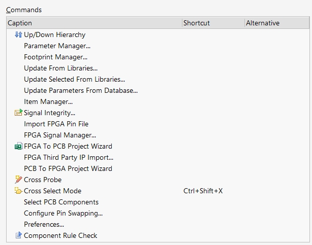
Underlined Connections: Commands related to managing or visualizing connections that may be implicitly created (e.g., power networks connected by port names).
Underlined Connections Commands Overview
These commands manage and visualize connections that are implicitly created through naming conventions rather than explicit wires, such as power networks connected by identical port names or net labels.
Individual Underlined Connection Commands:
Color-Coded Visualization:
Blue - Displays implicit connections with blue underlining
Light Green - Displays implicit connections with light green underlining
Light Blue - Displays implicit connections with light blue underlining
Red - Displays implicit connections with red underlining
Fuchsia - Displays implicit connections with fuchsia/magenta underlining
Yellow - Displays implicit connections with yellow underlining
Dark Green - Displays implicit connections with dark green underlining
What Are Underlined Connections:
Implicit Electrical Connections:
Power Ports: All GND symbols automatically connect to each other
Named Nets: Net labels with identical names create electrical connections
Off-Sheet Connectors: Connectors with same names across different sheets
Hierarchical Ports: Ports that connect between parent and child sheets
Visual Indication:
Underlined text or symbols show implicit connections exist
Color coding helps identify different types of implicit networks
Makes invisible electrical connections visible for verification
Essential for understanding complete circuit connectivity
Key Applications:
Power Network Visualization:
Red: Power supply connections (VCC, VDD, +5V)
Blue: Ground connections (GND, VSS, chassis ground)
Yellow: Negative supply voltages (-5V, -12V)
Green: Analog supply voltages (AVCC, AGND)
Signal Network Organization:
Light Blue: Clock and timing signals
Light Green: Data bus connections
Fuchsia: Control and enable signals
Dark Green: Test and debug connections
Multi-Sheet Design Verification:
Visualize connections that span multiple schematic sheets
Verify hierarchical connections between parent and child sheets
Identify all components connected to specific power rails
Trace signal paths across complex designs
Typical Usage:
Design Verification:
Select appropriate color for specific network type
Underlined connections become visible for that network class
Verify all intended connections are properly established
Identify missing or incorrect implicit connections
Network Analysis:
Use different colors to trace different types of implicit connections
Verify power distribution networks are complete
Check signal routing across multiple sheets
Validate hierarchical design connectivity
Documentation and Review:
Color-code different network types for design reviews
Make implicit connections visible in documentation
Help team members understand complete connectivity
Verify design intent is properly implemented
Benefits:
Design Verification: Ensures all implicit connections are intentional and correct
Visual Clarity: Makes invisible electrical connections visible
Error Prevention: Identifies unintended connections through naming conflicts
Multi-Sheet Coordination: Verifies connectivity across complex hierarchical designs
Professional Review: Enables thorough design verification and documentation
These Underlined Connection commands are essential for verifying the complete electrical connectivity in professional schematic designs, especially in complex multi-sheet projects where many connections exist through naming conventions rather than explicit wires.
View: Commands for managing display (Zoom In, Zoom Out, Show Entire Document, Grids, Show/Hide elements).
Let me explain the View commands in Altium Designer 2025: View Commands Overview These commands manage display control including zoom operations, document fitting, grid display, and show/hide interface elements for optimal schematic viewing and workspace management. Individual View Commands: Document and Object Fitting: Fit Document - Fits the entire schematic document in the viewing window Shows complete schematic sheet boundaries Useful for getting overall project overview Automatically adjusts zoom to show entire document Fit All Objects (Ctrl+PgDn) - Fits all schematic objects in the viewing window Shows only the area containing actual design elements Excludes empty sheet areas for efficient viewing Most commonly used fit command for design work Area - Fits a user-selected rectangular area in the view Click and drag to define specific area to view Precise zoom control for specific circuit sections Interactive area selection for detailed work Around Point - Centers view around a specific cursor point Click-to-center navigation Maintains current zoom level while recentering Quick navigation without zoom changes Selected Objects - Fits currently selected objects in the view Zooms to show only selected components or elements Useful for focusing on specific design elements Context-sensitive viewing for detailed editing Zoom Controls: Zoom In (PgUp) - Increases magnification for closer view Standard zoom-in for detailed work Keyboard shortcut for rapid zooming Centers zoom on current cursor position Zoom Out (PgDn) - Decreases magnification for broader view Standard zoom-out for overview perspective Quick access to see more of the design Maintains view center during zoom Zoom Last - Returns to the previous zoom level and position Undo last zoom operation Toggle between current and previous view states Useful for comparing different zoom levels Display Modes: Full Screen (Alt+F5) - Toggles full screen mode Maximizes schematic viewing area Hides all interface elements except design area Useful for presentations and detailed review work Show Net Color Override (F5) - Toggles net color highlighting display Shows/hides custom net color assignments Essential for viewing color-coded signal networks Toggle network visualization on/off PCB Release View - Shows schematic in PCB-ready view mode Displays schematic as it will appear for PCB transfer Shows component footprint information Validates PCB readiness before layout Workspace Management: Workspace (Ctrl+`) - Manages workspace configurations Controls panel arrangements and interface layout Switches between different workspace setups Customizes interface for different workflow phases Home - Returns to home/start screen Access to recent projects and templates Central navigation hub for Altium Designer Project selection and management interface Interface Elements: Status Bar - Shows/hides the status bar at bottom of interface Displays current tool information and coordinates Shows design statistics and system status Toggle for screen space optimization Command Status - Shows/hides command status information Displays active command and parameter information Shows current tool status and options Useful for understanding available operations Toggle Units - Switches between measurement units (mm/mil/inch) Changes display units for coordinates and measurements Critical for working with different design standards Switches between metric and imperial units Key Benefits: Navigation Efficiency: Rapid movement and zoom control for large designs Workspace Optimization: Customize interface for maximum productivity View Management: Multiple ways to control what's visible and how Professional Workflow: Support for different phases of design work These View commands are fundamental for efficient schematic design work, providing the navigation and display control necessary for working with complex electronic designs across different levels of detail.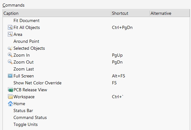
Window: Standard window management commands (Cascade, Tile, Switch Window).
Window Commands Overview
These are standard window management commands for organizing and switching between multiple open documents, providing efficient navigation when working with multiple schematics, PCBs, and other design files simultaneously.
Individual Window Commands:
Window Arrangement:
Tile (Shift+F4) - Tiles all open windows in a grid pattern
Arranges windows to show all documents simultaneously
Automatically sizes windows to fit available screen space
Useful for comparing multiple schematics or design files
Tile Horizontally - Arranges windows in horizontal strips
Stacks windows horizontally across the screen
Each window gets equal horizontal space
Good for comparing documents side-by-side vertically
Tile Vertically - Arranges windows in vertical columns
Stacks windows vertically across the screen
Each window gets equal vertical space
Ideal for side-by-side document comparison
Advanced Window Arrangement:
Arrange All Windows Horizontally - Comprehensive horizontal arrangement of all open windows
Arrange All Windows Vertically - Comprehensive vertical arrangement of all open windows
Document Management:
Close Documents - Closes the currently active document
Saves changes if prompted
Returns focus to next open document
Basic document lifecycle management
Close All - Closes all open documents at once
Prompts to save changes for all modified documents
Quick way to clear workspace
Useful when switching between projects
Quick Window Access:
View Window 1 through View Window 9 - Direct access to specific open windows
Each number corresponds to a specific open document
Quick switching between frequently used documents
Numbered based on opening order or usage
More Windows... - Opens comprehensive window list for additional management
Shows all open windows when more than 9 are open
Provides additional window management options
Extended window navigation capabilities
Key Applications:
Multi-Sheet Design:
Work on multiple schematic sheets simultaneously
Compare different design iterations
Cross-reference between related schematics
Maintain context across hierarchical designs
Cross-Domain Design:
View schematic and PCB documents simultaneously
Compare schematic with library documents
Work with simulation results alongside design files
Coordinate between different design domains
Team Collaboration:
Review multiple team member contributions
Compare design versions and revisions
Coordinate changes across multiple documents
Maintain awareness of project-wide changes
Typical Usage Workflows:
Design Review:
Open multiple related schematic sheets
Use Tile (Shift+F4) to view all sheets simultaneously
Compare circuits and verify consistency
Switch between windows using View Window 1-9
Hierarchical Design:
Open parent and child schematic sheets
Use Tile Vertically for side-by-side comparison
Verify hierarchical connections and interfaces
Maintain visual context of system architecture
Multi-Project Work:
Open documents from different projects
Use window switching for rapid context changes
Close All when switching between major projects
Use More Windows... for complex project management
Benefits:
Productivity: Efficient navigation between multiple open documents
Context Awareness: Maintain visual connection between related files
Comparison Capability: Side-by-side document comparison and analysis
Workflow Flexibility: Adapt window arrangement to current task requirements
These Window commands are essential for managing complex electronic design projects that involve multiple related documents, enabling efficient workflow management and maintaining design context across the entire project.
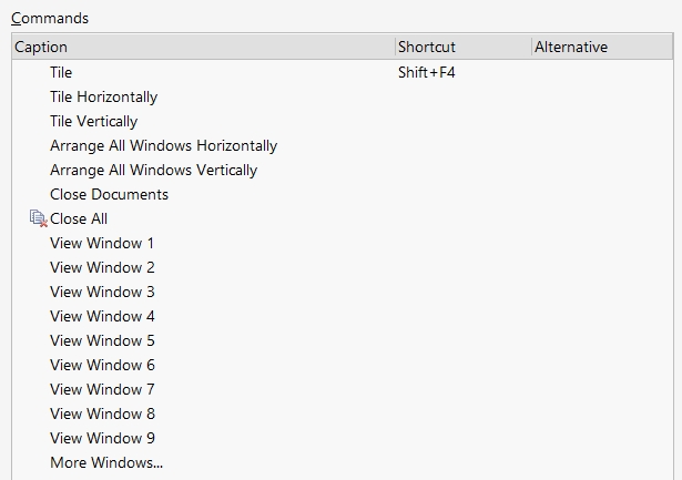
Wiring: Specific tools for placing electrical connections (Wires, Buses, Signal Harnesses).
Wiring Commands Overview
These are specific tools for placing electrical connections including wires, buses, signal harnesses, and power connections - the fundamental elements for creating electrical connectivity in schematic designs.
Individual Wiring Commands:
Basic Electrical Connections:
Wire (Ctrl+W) - Places individual wires for point-to-point connections
Most fundamental schematic connection tool
Creates electrical connections between component pins
Essential for all circuit connectivity
Supports automatic junction creation
Bus - Places multi-wire buses for grouped signal connections
Represents multiple related signals as single thick line
Used for data buses, address buses, control signal groups
Reduces visual clutter in digital designs
Common for 8-bit, 16-bit, or 32-bit data paths
Bus Management:
Bus Joiner - Connects multiple buses together
Joins separate bus segments into continuous networks
Essential for complex bus routing
Maintains electrical connectivity across bus splits
Bus Entry - Creates connection points between individual wires and buses
Allows individual signals to connect to or branch from buses
Maintains clean visual representation of bus connections
Critical for accessing individual signals from grouped buses
Network Identification:
Net Label - Places text labels to identify and name electrical networks
Names electrical connections for clarity and cross-sheet connectivity
Enables connections across multiple schematic sheets
Essential for multi-sheet and hierarchical designs
Power Connections:
Place GND power port - Places ground connection symbols
Standard ground reference connections
Automatically connects all GND symbols project-wide
Place GND Bus power port - Places ground connections for bus-style power distribution
Bus-oriented ground connections for multi-rail systems
Used in complex power distribution designs
Place VCC power port - Places positive power supply connections
Standard positive supply voltage connections
Automatically connects all VCC symbols project-wide
Place VCC Bus power port - Places VCC connections for bus-style power distribution
Bus-oriented power connections for multi-rail systems
Used in complex power management designs
Component Integration:
Part... - Places components from libraries onto the schematic
Primary tool for adding electronic components
Links to component libraries and databases
Foundation for all circuit design
Hierarchical Design Elements:
Sheet Symbol - Places hierarchical sheet symbols for modular design
Represents entire child schematic sheets as symbols
Essential for complex, multi-sheet designs
Enables system-level design organization
Sheet Entry - Creates connection points on sheet symbols
Defines electrical interfaces between hierarchical levels
Critical for maintaining connectivity across design hierarchy
Device Sheet Symbol - Places device-specific sheet symbols
Specialized sheet symbols for specific hardware devices
Used for complex ICs requiring detailed internal representation
Embedded System Integration:
C Code Symbol - Places embedded code symbols for software integration
Represents software components in hardware designs
Links hardware and software design elements
Add C Code Entry - Adds entries to code symbols
Creates interface points between hardware and software
Essential for embedded system design
Harness and Cable Design:
Signal Harness - Creates signal harnesses for cable design
Groups multiple wires into cable assemblies
Essential for automotive, aerospace, and industrial designs
Represents multi-conductor cables and wire bundles
Harness Connector - Places connectors for harness designs
Multi-pin connectors for cable assemblies
Defines harness entry and exit points
Harness Entry - Creates entry points for harness connections
Connection points where individual wires join harnesses
Maintains clean harness representation
Interface Connections:
Port - Places hierarchical connection ports
Enables connections between different hierarchical levels
Essential for modular design methodology
Key Applications:
Circuit Connectivity: All electrical connections between components
Power Distribution: Clean power and ground connection management
Bus Systems: Organized multi-signal connections for digital designs
Hierarchical Design: Modular circuit organization and interfaces
Cable Design: Wire harness and multi-conductor cable representation
Typical Workflow:
Place Part... components from libraries
Use Wire (Ctrl+W) to connect component pins
Add Power Ports for power and ground connections
Use Bus and Bus Entry for grouped digital signals
Add Net Label to name important signals
Use Sheet Symbol and Port for hierarchical organization
These Wiring commands form the foundation of schematic design, providing all the tools necessary to create complete electrical connectivity in professional electronic designs.
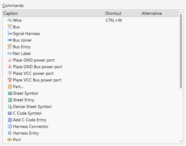
This is a fairly complete overview of the command categories available in the Altium Designer schematic editor. Each of these categories contains many individual commands that can be added to toolbars or menus for quick access.