PCB Editor
Advanced board layout environment with precision placement and routing tools for translating schematics into manufacturable PCB designs.
Advanced board layout environment with precision placement and routing tools for translating schematics into manufacturable PCB designs.
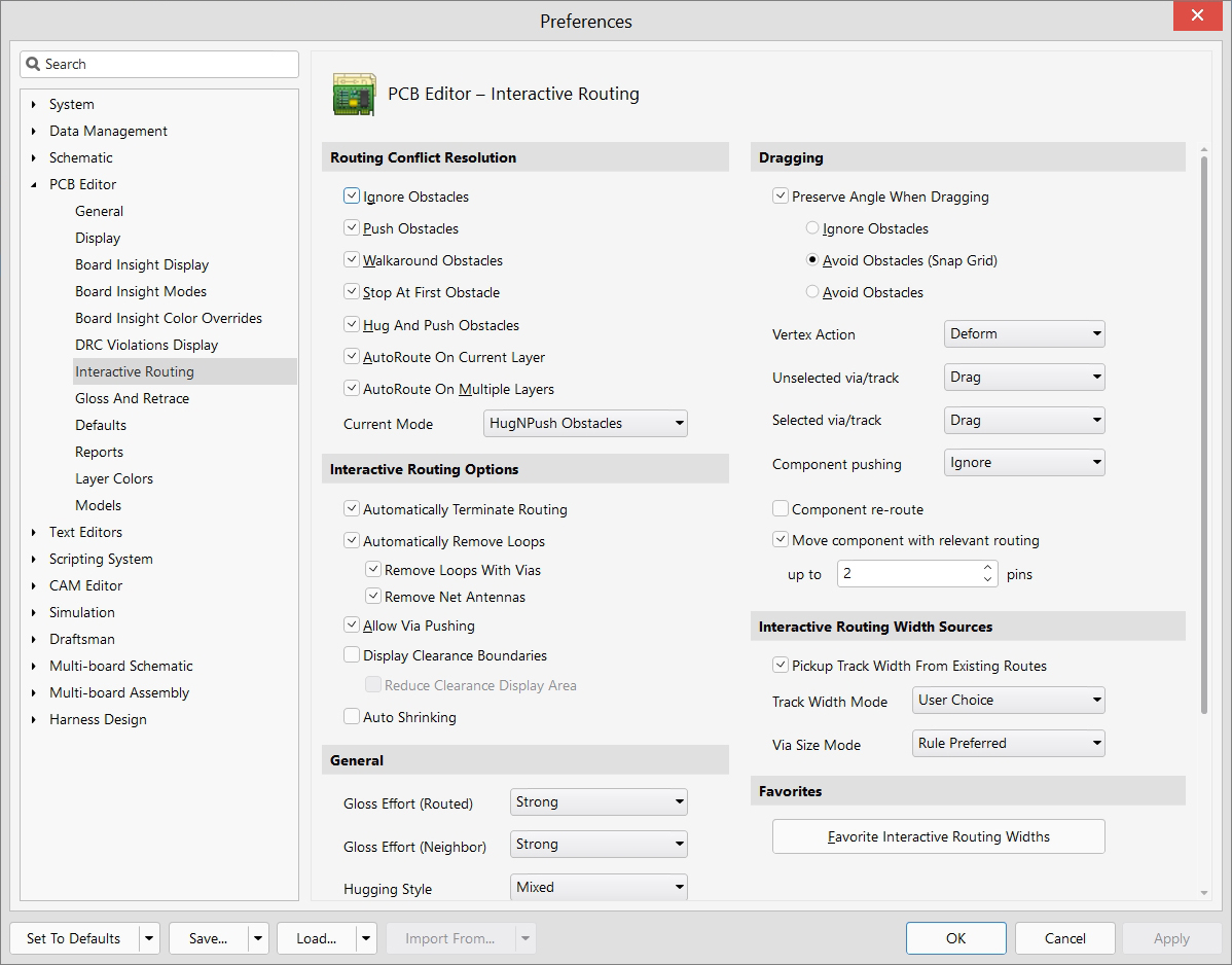
The PCB Editor in Altium Designer 2025 is a comprehensive tool for designing and developing printed circuit boards with an extensive set of features.
Directly linked to Schematic Editor through synchronization mechanism. Uses data from Component Library Manager for component placement. Interacts with Design Rule Checker for design rule verification. Integrates with Manufacturing Integration for preparing production data
| Term | Definition |
|---|---|
| Board Outline | The physical boundary or shape of the PCB, defining its mechanical dimensions and form factor |
| Clearance | The minimum required distance between conductive elements on a PCB to prevent electrical shorts |
| Copper Pour | A large area filled with copper on a PCB layer, typically connected to a ground or power net to provide shielding and improved current flow |
| Design Rules | A set of constraints and parameters defining manufacturing limitations such as minimum trace width, spacing, and hole sizes |
| Differential Pair | Two traces routed closely together carrying equal and opposite signals for improved noise immunity and signal integrity |
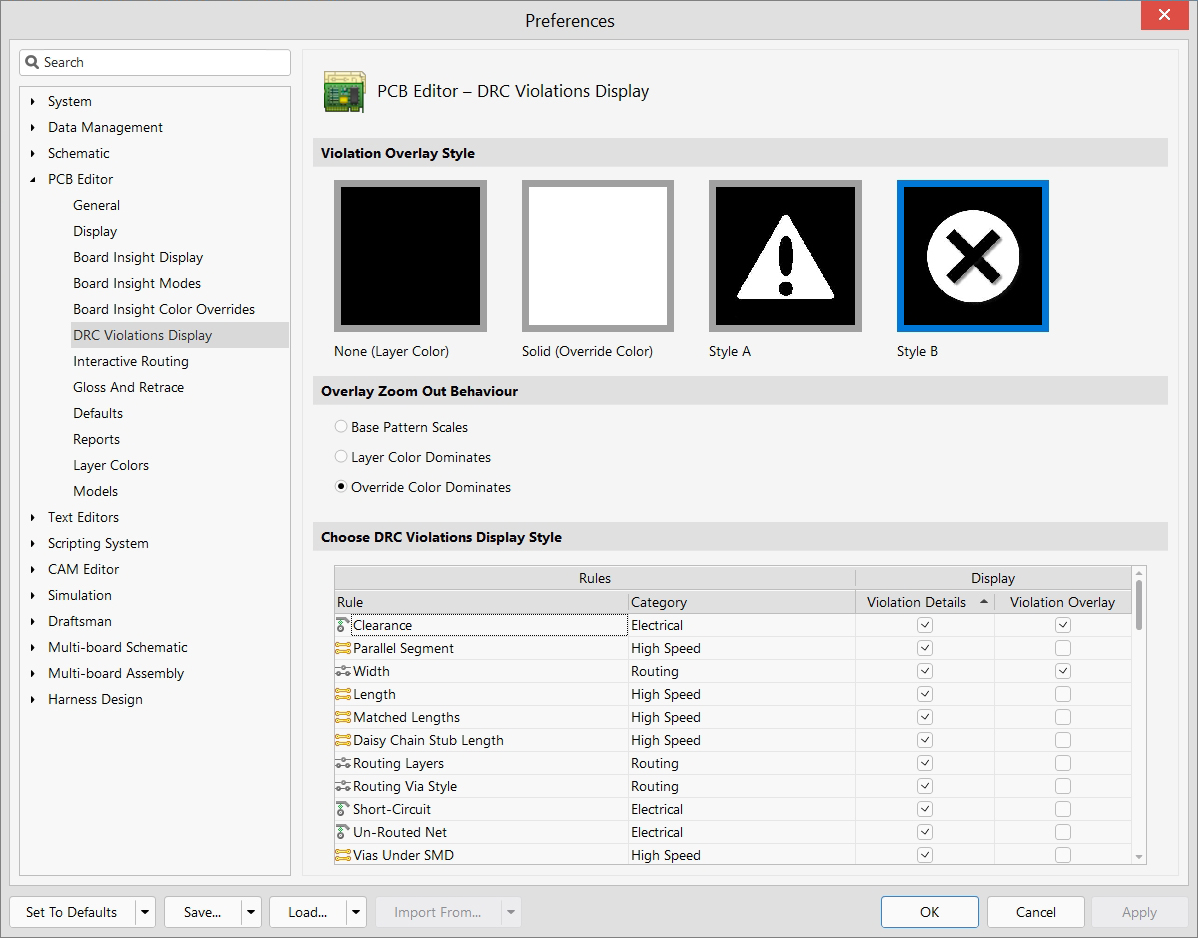
| DRC (Design Rule Check) | Automated verification process that ensures the PCB design meets manufacturing and electrical requirements |
| Drill | Process of creating holes in the PCB for through-hole components, vias, or mounting points |
| Fanout | Pattern of traces and vias that distribute connections from densely packed component pads (such as BGAs) to less congested areas |
| Footprint | The pattern of pads and silk screen information that represents a physical component on the PCB |
| Gerber | Standard file format used for PCB manufacturing that describes the conductive and non-conductive layers |
| Grid | A visible or invisible coordinate system used for precise placement and alignment of elements in the PCB layout |
| Keepout | An area on the PCB where routing or component placement is prohibited due to mechanical or electrical constraints |
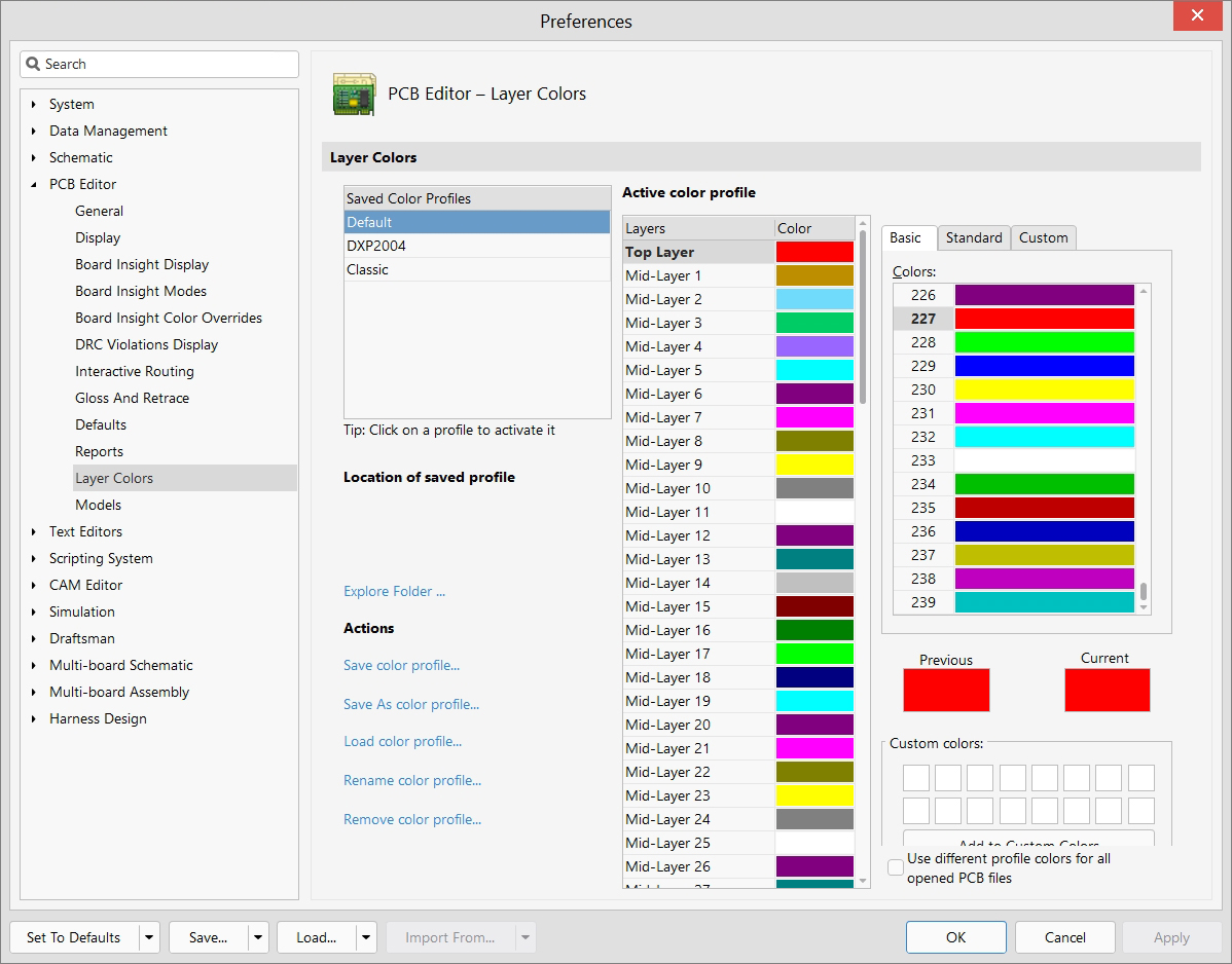
| Layer Stack | The arrangement and composition of the PCB's conductive and insulating layers, defining its structure |
| Length Matching | Technique of making traces the same length to ensure signals arrive simultaneously, critical for high-speed interfaces |
| Net | A set of electrically connected pins and traces in the PCB that forms a single electrical connection |
| Pad | A conductive area on the PCB where component leads or pins are soldered |
| Panelization | Process of arranging multiple PCB designs on a single manufacturing panel for efficient production |
| Paste Mask | Layer defining areas where solder paste should be applied during the assembly process for surface mount components |
| Pick and Place | Data file containing component positions and orientations used by automated assembly equipment to place components |
| Placement | The process of positioning components on the PCB according to design requirements and constraints |
| Plane | A solid copper area that spans most of a PCB layer, typically used for power distribution or grounding |
| Polygon | A multi-sided copper shape used for conductor areas, shields, or power distribution |
| Primitive | Basic geometric shape used in PCB design such as line, arc, fill, or text |
| Ratlines | Visual indicators showing electrical connections that need to be routed between component pins |
| Route | The process of creating conductive paths between components according to the circuit schematic |
| Silkscreen | Non-conductive layer on the PCB surface containing text, component outlines, and reference designators |
| Snap | Feature that automatically aligns objects to a grid or other elements to ensure precise placement |
| Teardrop | Smoothed connection between a trace and pad that strengthens the junction and improves manufacturing reliability |
| Track (Trace) | A conductive path on the PCB that carries electrical signals between components |
| Via | A plated hole that connects traces between different layers of the PCB |