Glossary of terms

PCB Routing and Layout

Sophisticated routing technologies that streamline board layout while maintaining signal integrity for even the most complex designs.

Revolutionary routing technologies that combine intelligent algorithms with engineering precision.

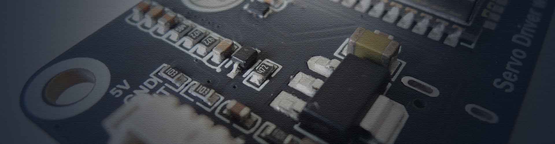
PCB Routing and Layout tools in Altium Designer 2025 represent a comprehensive suite of advanced technologies designed to streamline the board layout process while maintaining optimal signal integrity. These sophisticated routing capabilities enable engineers to tackle even the most complex designs with confidence and efficiency.

Overview

The PCB routing and layout system in Altium Designer combines intelligent automation with precise manual control, providing designers with the flexibility to choose the best approach for each unique challenge. From basic two-layer boards to complex multi-layer designs with thousands of connections, these tools ensure professional results every time.


Core Technologies


Push & Shove Routing

Interactive routing technology that dynamically adjusts existing traces as you route new connections.

  • Real-time obstacle resolution - Automatically pushes existing routes aside to make room for new traces
  • Design rule compliance - Maintains clearances and constraints while routing
  • Smooth trace optimization - Creates clean, manufacturable routing patterns
  • Multi-layer support - Works seamlessly across all board layers


  • ActiveRoute (AI-assisted routing)

  • Artificial intelligence - powered routing that learns from your design patterns to accelerate layout completion.
  • Machine learning algorithms - Analyzes your routing style and applies it automatically
  • Guided routing - Suggests optimal paths based on design constraints
  • Batch routing - Routes multiple connections simultaneously
  • Quality optimization - Balances routing density with signal integrity


  • Differential Pair Routing

    Specialized tools for routing high-speed differential signals with precise control.

  • Automatic pair matching - Maintains consistent spacing between differential traces
  • Length matching - Ensures equal trace lengths for optimal signal timing
  • Impedance control - Maintains target impedance throughout the routing path
  • Phase tolerance management - Controls timing skew between paired signals


  • Length Tuning

    Advanced trace length matching for high-speed designs and timing-critical signals.

  • Accordion patterns - Automatically creates serpentine routes for length adjustment
  • Visual feedback - Real-time display of length differences and target values
  • Group tuning - Match multiple nets simultaneously
  • Tolerance control - Set precise matching requirements for different signal groups


  • Gloss & Optimize

    Automated cleanup tools that refine your routing for improved manufacturability.

  • Trace smoothing - Removes unnecessary bends and jogs
  • Via optimization - Minimizes via count and improves signal quality
  • Angle correction - Converts traces to preferred angles (45° or 90°)
  • Spacing optimization - Maximizes clearances where possible


  • Design Reuse Blocks

    Leverage proven circuit sections to accelerate new designs and ensure consistency.

  • Modular approach - Save complete routed sections as reusable blocks
  • Intelligent placement - Automatically adapts blocks to new board layouts
  • Connection preservation - Maintains routing patterns and relationships
  • Version management - Track and update reused blocks across projects
  • Key Benefits


    Increased Productivity

  • Reduce routing time by up to 80% with intelligent automation
  • Focus on critical areas while automation handles routine connections
  • Batch operations for repetitive tasks

  • Signal Integrity

  • Built-in high-speed design rules ensure optimal performance
  • Real-time impedance calculations
  • Automatic length matching for timing-critical signals

  • Design Quality

  • Consistent routing patterns across the entire board
  • Automated design rule checking during routing
  • Professional, manufacturable results

  • Flexibility

  • Seamlessly switch between manual and automated routing
  • Customizable routing strategies for different design areas
  • Support for all board technologies from simple to HDI

  • Integration with Design Flow

    PCB Routing and Layout tools are deeply integrated with other Altium Designer features:

  • Schematic synchronization - Automatic updates from schematic changes
  • 3D visualization - Real-time 3D view during routing
  • Design rule system - Comprehensive constraint management
  • Manufacturing checks - Built-in DFM verification

  • Best Practices

  • Define clear design rules before starting routing
  • Use hierarchy to organize complex designs
  • Leverage automation for initial routing, then refine manually
  • Regularly run design rule checks during the routing process
  • Utilize design reuse for proven circuit sections

  • Summary

    Altium Designer's PCB Routing and Layout tools provide the perfect balance of automation and control, enabling designers to create high-quality boards efficiently. Whether you're working on a simple two-layer design or a complex HDI board with thousands of connections, these tools adapt to your needs while maintaining the highest standards of signal integrity and manufacturability.


    PCB Routing and Layout in ECAD-MCAD